Periodic metal contact gain-coupled distributed feedback semiconductor laser device

A technology of metal contact and gain coupling, applied in the structure of optical waveguide semiconductors, etc., can solve the problems of complex technology and difficult cost, and achieve the effects of simple manufacturing process, reduced manufacturing cost, and good side mode suppression ratio

Inactive Publication Date: 2016-07-27
CHANGCHUN INST OF OPTICS FINE MECHANICS & PHYSICS CHINESE ACAD OF SCI
View PDF2 Cites 8 Cited by
  • Summary
  • Abstract
  • Description
  • Claims
  • Application Information

AI Technical Summary

Problems solved by technology

[0005] In order to solve the problems existing in the prior art, the present invention provides a periodic metal contact gain-coupling distributed feedback semiconductor laser, which mainly solves the problem that the existing scheme of semiconductor laser single longitudinal mode operation is complex, precise, costly and difficult to be practical

Method used


Image

  • Periodic metal contact gain-coupled distributed feedback semiconductor laser device
  • Periodic metal contact gain-coupled distributed feedback semiconductor laser device
  • Periodic metal contact gain-coupled distributed feedback semiconductor laser device

Examples


Embodiment 1

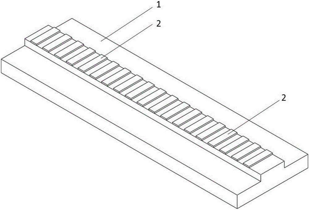
[0029] Such as figure 1 As shown, in this example,

[0030] On the designed and prepared GaAs-based semiconductor laser chip 1 with a wavelength of λ and an effective refractive index n in this wavelength band, a ridge-shaped mesa is prepared at one time by photolithography and etching. The width of the mesa is 100 μm and the height is 1.4 μm. . Deposit 200nm thick SiO 2 Insulation. Then, periodic electrode openings are prepared by overlaying. The opening period δ is: δ=Mλ / 2n, where M is a positive integer greater than 2. In this embodiment, when n=3.48, λ=980 nm, M=40, then δ=5.632 μm. The width of each electrode strip is 1.5 μm. Etching off SiO by means of ohmic contact 2 P-surface electrodes are evaporated on the electrode strips. Since only periodic electrodes have metal contacts, the preparation of periodic metal contacts 2 is completed. The required periodic metal contact gain coupling distribution feedback semiconductor laser single tube device is obtained throug...

Embodiment 2

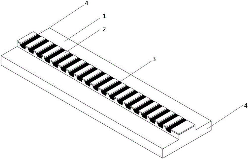
[0032] Such as figure 2 As shown, in this example,

[0033] In the already designed and prepared λ 1 and lambda2 All wavelengths have optical gain, and the effective refractive index in this band is n 1 and n 2 On the InP-based semiconductor laser chip 1, a ridge-shaped mesa was prepared at one time by photolithography and etching, with a mesa width of 4 μm and a height of 1.86 μm. The lateral current confinement region 3 is prepared by oxidation or carrier injection, and the electrode period δ is: δ=M i λ / 2n, i takes 1 or 2, M i is a positive integer greater than 2, and n is the effective refractive index of the semiconductor laser waveguide in this band. In this example, when n 1 =3.16,λ 1 =1550nm, take M 1 =80, then δ=19.62μm, there are n in this cycle 2 =3.15,λ 2 =1526nm, M 2 =81. The width of each electrode is 15 μm. Deposit 200nm thick SiO 2 Insulation. Periodic metal contacts 2 are fabricated by overlaying, etching and ohmic contact. The required period...

Embodiment 3

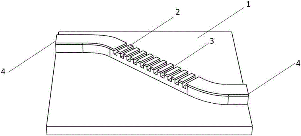
[0035] Such as image 3 As shown, in this example,

[0036] In the already designed and prepared λ 1 and lambda 2 All wavelengths have optical gain, and the effective refractive index in this band is n 1 and n 2 On the GaAs-based quantum dot semiconductor laser chip 1, a ridge-shaped mesa with a curved waveguide is etched at one time by photolithography and etching. The width of the mesa is 6 μm and the height is 1.4 μm. By bending the waveguide, the resonance direction of the periodic metal contact gain-coupling distributed feedback semiconductor laser is adjusted to the crystal orientation with high nonlinear coefficient. Optical grooves are prepared by overlaying and etching for the lateral current confinement region 3, and the electrode period δ is: δ=M i λ / 2n, i takes 1 or 2, M i is a positive integer greater than 2, and n is the effective refractive index of the semiconductor laser waveguide in this band. In this example, when n 1 =3.28,λ 1 = 1300nm, take M 1 =...


PUM


Abstract

The invention provides a periodic metal contact gain-coupled distributed feedback semiconductor laser device, belongs to the technical field of semiconductor laser chips, and aims at solving the problems that the distributed feedback semiconductor laser device in the prior art is difficult to prepare and high in cost. Periodic metal contacts are manufactured on a semiconductor laser chip; lateral current restricted areas can be manufactured between the periodic metal contacts through means of etching, oxidization, current carrier injection and the like; and high-reflective films or antireflective films can also be manufactured on the end surfaces of the chip. According to the periodic metal contact gain-coupled distributed feedback semiconductor laser device, semiconductor laser single-tube or linear array output with high power and narrow linewidth can be achieved; and the periodic metal contact gain-coupled distributed feedback semiconductor laser can also be applied to other semiconductor laser devices as a seed source, or can be applied to generation of a dual-wavelength or frequency comb-excited semiconductor laser light, or is used for carrying out nonlinear optical effect, and can also be used for obtaining a semiconductor laser pump light source with a stable wavelength.

Description

technical field [0001] The invention belongs to the technical field of novel semiconductor lasers, in particular to a periodic metal contact gain coupling distributed feedback semiconductor laser. Background technique [0002] Traditional semiconductor lasers are currently widely used in industrial processing, medical treatment, communications, national defense, pump sources and other fields. However, due to the large wavelength drift of semiconductor lasers with current injection and the difficulty in achieving single longitudinal mode operation, they cannot meet the needs of many application fields. [0003] In order to solve the problem of regulating the longitudinal mode and line width of semiconductor lasers, the methods commonly used at present are: distributed feedback lasers using refractive index coupling and phase shift gratings, semiconductor lasers using high-order distributed Bragg reflection gratings, and injection-locked semiconductor lasers. lasers and exter...

Claims


Application Information

Patent Timeline
IPC IPC(8): H01S5/22
CPCH01S5/22
Inventor 陈泳屹贾鹏秦莉宁永强王立军
Owner CHANGCHUN INST OF OPTICS FINE MECHANICS & PHYSICS CHINESE ACAD OF SCI
Why Eureka
Try Eureka