High-performance low-cost DFB laser epitaxial wafer and manufacturing method thereof

A DFB laser and manufacturing method technology, which is applied to lasers, laser parts, semiconductor lasers, etc., can solve the problem that the holographic exposure uniformity has a large influence on the optical path, the DFB laser yield has a large influence, and it is difficult to achieve large-size uniform gratings, etc. problem, to achieve the effect of suppressing the spatial hole burning effect, improving the side mode suppression ratio, and achieving excellent performance.

Pending Publication Date: 2022-03-11
全磊光电股份有限公司
View PDF3 Cites 0 Cited by
  • Summary
  • Abstract
  • Description
  • Claims
  • Application Information

AI Technical Summary

Problems solved by technology

[0004] The traditional grating is distributed in the whole resonant cavity, so there will be two modes randomly distributed, the double peak effect is obvious, and the wavelength stability is poor
[0005] Invention patent CN201710632079.3, using double exposure method to prepare asymmetric grating, first use holographic coherent exposure method to expose with ultraviolet lithography machine, after the two exposures are completed, use developer to develop, and then use corrosion solution to grating area Etching is carried out simultaneously with the non-grating area, and then the photoresist mask is removed; however, the area in contact with the solution between the grating area and the non-grating area is quite different, and the etching rate of the two positions is significantly different during etching, and the two areas cannot be reached at the same time. Just in the state of complete etching, the non-grating area has the problem of too deep etching. After the second epitaxy, it will affect the reliability of the device. The uniformity of holographic exposure is greatly affected by the optical path, and it is difficult to achieve a large-scale uniform grating. Great impact on DFB laser yield

Method used


Image

  • High-performance low-cost DFB laser epitaxial wafer and manufacturing method thereof
  • High-performance low-cost DFB laser epitaxial wafer and manufacturing method thereof
  • High-performance low-cost DFB laser epitaxial wafer and manufacturing method thereof

Examples


Embodiment

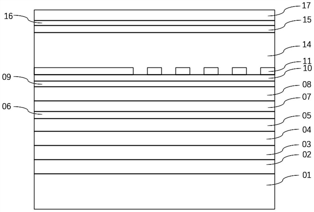
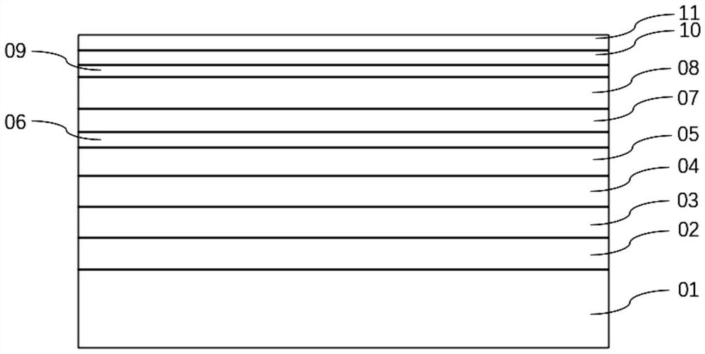
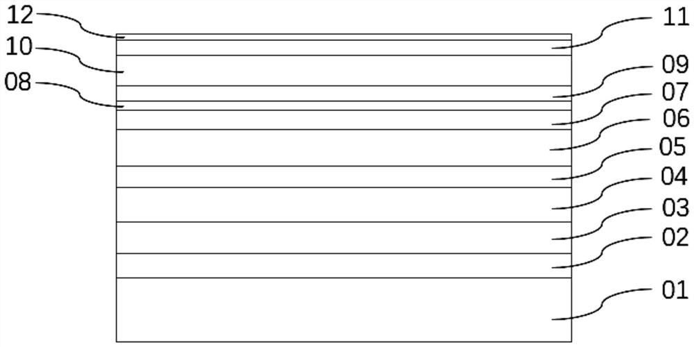
[0041] Example: such as figure 1 As shown, a high-performance and low-cost DFB laser epitaxial wafer, including a substrate 01, a lower buffer layer 02, a lower confinement layer 03, a lower waveguide layer 04, a quantum well 05, and an upper waveguide layer 06, which are sequentially stacked from bottom to top , upper confinement layer 07, upper buffer layer 08, corrosion barrier layer 09, cladding layer 10, grating fabrication layer 11, secondary epitaxial layer 14, barrier gradient layer and ohmic contact layer 17; grating fabrication layer 11 is divided into grating area and non-raster area. The area of ​​the grating area is larger than the area of ​​the non-grating area. The thickness of the grating fabrication layer 11 is 40 nm, and the grating region of the grating fabrication layer 11 has an asymmetric grating structure. The substrate 01 is an InP substrate, the lower buffer layer 02 is an N-InP layer, the lower confinement layer 03 is an N-AlInAs layer, the lower wa...

specific Embodiment

[0051] With a conductivity of 2-8x10 18 cm -2 InP is used as the growth substrate and put into the MOCVD system for growth. The reaction chamber pressure was 50mbar, the growth temperature was 670°C, and the 2 As carrier gas, trimethylindium (TMIn), trimethylgallium (TMGa), trimethylaluminum (TMAl), diethylzinc (DeZn), silane (SiH 4 ), arsine (AsH 3 ) and phosphine (PH 3 ) etc. as the reaction source gas, sequentially grow N-InP buffer layer, N-AlInAs confinement layer, non-doped AlGaInAs lower waveguide layer with graded refractive index, 6-period AlGaInAs quantum wells, non-doped graded refractive index AlGaInAs upper waveguide layer, non-doped AlInAs confinement layer, P-InP transition layer, InGaAsP corrosion barrier layer with wavelength of 1100nm, InP cladding layer and InGaAsP grating fabrication layer with wavelength of 1100nm. The thickness of the InGaAsP grating fabrication layer is 40 nm.

[0052] Spin-coat a photoresist mask on the surface of the above-mentio...


PUM

PropertyMeasurementUnit
thicknessaaaaaaaaaa
wavelengthaaaaaaaaaa

Abstract

A high-performance low-cost DFB laser epitaxial wafer comprises a substrate, a lower buffer layer, a lower limiting layer, a lower waveguide layer, a quantum well, an upper waveguide layer, an upper limiting layer, an upper buffer layer, a corrosion barrier layer, a cladding, a grating manufacturing layer, a secondary epitaxial layer, a barrier gradient layer and an ohmic contact layer which are sequentially stacked from bottom to top. The grating manufacturing layer is divided into a grating area and a non-grating area. The invention provides a high-performance low-cost DFB laser epitaxial wafer and a manufacturing method thereof. The high-performance low-cost DFB laser epitaxial wafer can effectively restrain the space hole burning effect of a laser, improve the side mode rejection ratio of the DFB laser, optimize the spectral mode of the DFB laser, reduce the manufacturing requirement of a grating photoetching plate, improve the product yield of the DFB laser, and is low in manufacturing cost.

Description

technical field [0001] The invention relates to a laser epitaxial wafer and a manufacturing method thereof, in particular to a high-performance and low-cost DFB laser epitaxial wafer and a manufacturing method thereof. Background technique [0002] The optical communication network uses light as the carrier of signal transmission. Compared with the electrical communication network using copper cables as the transmission medium, the speed, capacity and anti-interference ability of information interconnection have been significantly improved, so it has been widely used. Semiconductor lasers are the main light sources for optical communication networks, including Fabry-Perot lasers (FP lasers), distributed feedback lasers (DFB) and vertical cavity surface emitting lasers (VCSEL). Among them, the DFB laser establishes a Bragg grating inside the semiconductor, and relies on the distribution feedback of light to realize the selection of a single longitudinal mode. In the current ...

Claims


Application Information

Patent Timeline
Patent Type & Authority Applications(China)
IPC IPC(8): H01S5/12H01S5/34H01S5/343
CPCH01S5/1228H01S5/1231H01S5/3421H01S5/34346
Inventor 李洪雨张双翔张永单智发
Owner 全磊光电股份有限公司
Why Eureka
Try Eureka