Semiconductor laser and optical fiber coupling structure

A fiber coupling and semiconductor technology, which is applied in the field of semiconductor laser devices, can solve the problems of reducing the electro-optical efficiency of semiconductor lasers, low chip output power density, and reducing the effect of space hole burning, etc., to achieve small size, light weight, and reduced quantity. Effect

Inactive Publication Date: 2021-04-06
INST OF APPLIED ELECTRONICS CHINA ACAD OF ENG PHYSICS
View PDF2 Cites 1 Cited by
  • Summary
  • Abstract
  • Description
  • Claims
  • Application Information

AI Technical Summary

Problems solved by technology

Since the resonant cavity is asymmetrical, the laser power density inside the chip is non-uniformly distributed, gradually increasing from HR to AR, which will lead to serious spatial hole burning effect, and this effect will increase and decrease with the increase of laser cavity length Electro-optic Efficiency of Semiconductor Lasers
[0006] At present, the problems of low chip output power density and spatial hole burning effect reducing the chip's electro-optical conversion efficiency in 790nm semiconductor lasers need to be solved

Method used


Image

  • Semiconductor laser and optical fiber coupling structure
  • Semiconductor laser and optical fiber coupling structure

Examples


Embodiment 1

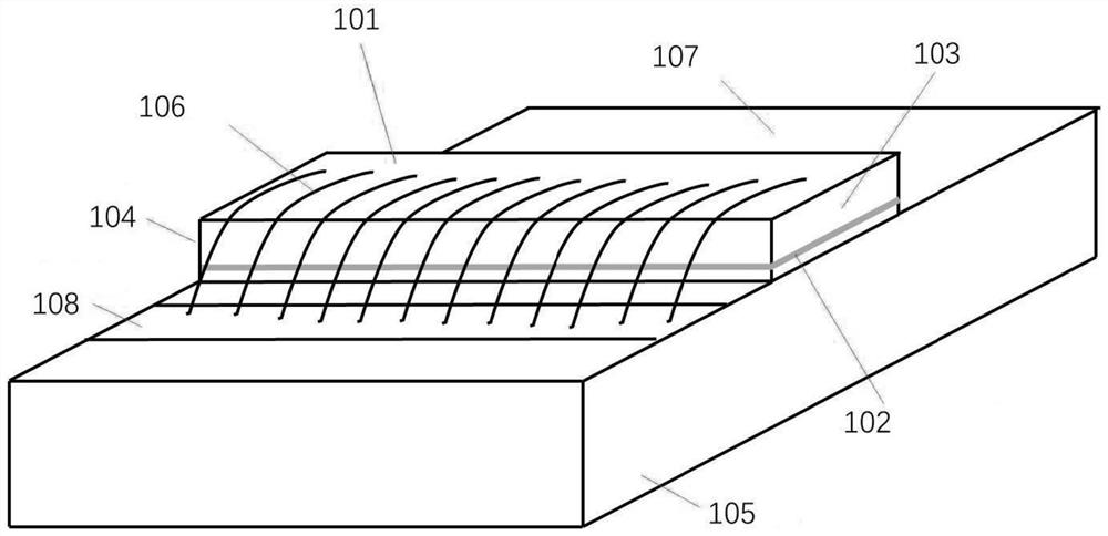
[0035] Such as figure 1 As shown, a semiconductor laser 201 is specifically provided in this embodiment, aiming at improving the total laser output power by optimizing and improving the semiconductor laser 201 . The semiconductor laser in this embodiment includes: a semiconductor laser chip 101 , and in this embodiment, the semiconductor laser chip 101 is a 790nm semiconductor laser chip 101 .

[0036] The semiconductor laser chip 101 is provided with two light-emitting surfaces, respectively the first light-emitting surface 103 and the second light-emitting surface 104, the first light-emitting surface 103 and the second light-emitting surface 104 are symmetrically arranged and the first light-emitting surface 103 and the second light-emitting surface The reflectivity of 104 is set equal, and the semiconductor laser chip 101 outputs laser beams from the first light-emitting surface 103 and the second light-emitting surface 104 respectively.

[0037] The advantage of the desi...

Embodiment 2

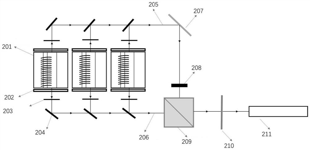
[0041] Such as figure 2 As shown, a fiber coupling structure is specifically provided in this embodiment, aiming to improve the electro-optical conversion efficiency of the chip and reduce the number of semiconductor laser chips 101 in the coupling structure through the fiber coupling structure. The fiber-coupled structure includes:

[0042]A plurality of semiconductor lasers 201 are arranged in an array, and each semiconductor laser 201 is equidistantly arranged in parallel along the same direction. Each of the semiconductor lasers 201 adopts the improved 790nm semiconductor laser 201 in Embodiment 1.

[0043] The laser beams output by the first light-emitting surface 103 of each of the semiconductor lasers 201 respectively pass through the fast-axis collimating mirror FAC202, the slow-axis collimating mirror SAC203 and the step mirror 204 arranged in sequence to generate first parallel beams 205 with different heights; The laser beam output by the second light-emitting sur...


PUM

PropertyMeasurementUnit
lengthaaaaaaaaaa
reflectanceaaaaaaaaaa

Abstract

The invention discloses a semiconductor laser and an optical fiber coupling structure, which belong to the technical field of semiconductor laser devices. The reflectivity of two cavity surfaces of a semiconductor laser chip is set to be equal, and laser is respectively output from a first light emitting surface and a second light emitting surface; a plurality of semiconductor lasers are arranged, the laser output from the first light emitting surface passes through respective lens assemblies to generate a first parallel light beam, and the laser output from the second light emitting surface passes through respective lens assemblies to generate a second parallel light beam; the first parallel light beam and the second parallel light beam simultaneously pass through the polarization beam combiner and the focusing lens after passing through the reflector and the half-wave plate and then are focused on the optical fiber, and laser is output from the two end faces of the laser chip and is of a symmetrical resonant cavity structure, so that the electro-optical conversion efficiency of the chip is improved, and the cavity surface power density is reduced; the total laser output power of a single laser chip can be improved; the optical fiber coupling structure reduces the number of chips, and is simpler and lighter in structure, small in size, light in weight and low in material consumption.

Description

technical field [0001] The invention belongs to the technical field of semiconductor laser devices, and in particular relates to a semiconductor laser and an optical fiber coupling structure. Background technique [0002] Semiconductor lasers are widely used in pumping solid-state and fiber lasers, material processing, and laser medical treatment due to their advantages such as compact structure, low cost, and easy control of the optical field. Among them, semiconductor lasers with a wavelength near 790nm are mainly used to pump Tm-doped fiber lasers, which can generate 2um infrared lasers. [0003] Due to the high photon energy of semiconductor lasers near 790nm, the cavity surface is prone to damage (COD). The (Al)GaInP / GaAsP structure without aluminum active region can effectively suppress the generation of dark line defects and reduce non-radiative recombination centers; The recombination rate increases the optical damage threshold of the cavity surface. [0004] Howev...

Claims


Application Information

Patent Timeline
Patent Type & Authority Applications(China)
IPC IPC(8): H01S5/10H01S5/024H01S5/042H01S5/40
CPCH01S5/02476H01S5/10H01S5/4012H01S5/04257
Inventor 周坤杜维川李弋吴华玲何林安高松信唐淳郭林辉
Owner INST OF APPLIED ELECTRONICS CHINA ACAD OF ENG PHYSICS
Why Eureka
Try Eureka