A semiconductor laser structure

A technology of lasers and semiconductors, which is applied in the direction of semiconductor lasers, optical waveguide semiconductor structures, lasers, etc., can solve the problems of increased internal loss of lasers, increased fast-axis far-field divergence angle, increased device threshold current, etc., to improve output Effects of power and efficiency, increasing fundamental mode limit factor, and reducing threshold current

Active Publication Date: 2022-03-15
INST OF APPLIED ELECTRONICS CHINA ACAD OF ENG PHYSICS
View PDF8 Cites 0 Cited by
  • Summary
  • Abstract
  • Description
  • Claims
  • Application Information

AI Technical Summary

Problems solved by technology

However, the waveguide structure with a large optical cavity reduces the confinement factor of the fundamental mode, which leads to an increase in the threshold current of the device and reduces the electrical-to-optical conversion efficiency of the laser; on the other hand, the increase in the optical cavity will definitely increase the mode in the waveguide structure. Higher-order modes may appear and lase in a large optical cavity, resulting in an increase in the fast-axis far-field divergence angle and degradation of beam quality, and the loss of the higher-order modes in the waveguide is higher than that of the fundamental mode in the waveguide, thus making the laser’s Increased internal loss is not conducive to the increase of laser output power, resulting in a decrease in the external quantum efficiency of the device
The traditional method adjusts the confinement factors of the fundamental mode and higher-order modes by adjusting the position of the quantum well in the waveguide. However, due to the large number of modes in the large optical cavity structure, the control effect of this method is limited, and the experimental repeatability is poor.
[0005] In summary, the confinement factor of the fundamental mode in the 790nm semiconductor laser with a large optical cavity waveguide structure is low, and the mode gain of the high-order mode is large, which is very unfavorable for the preparation of high-performance high-power semiconductor lasers

Method used


Image

  • A semiconductor laser structure
  • A semiconductor laser structure
  • A semiconductor laser structure

Examples


Embodiment 1

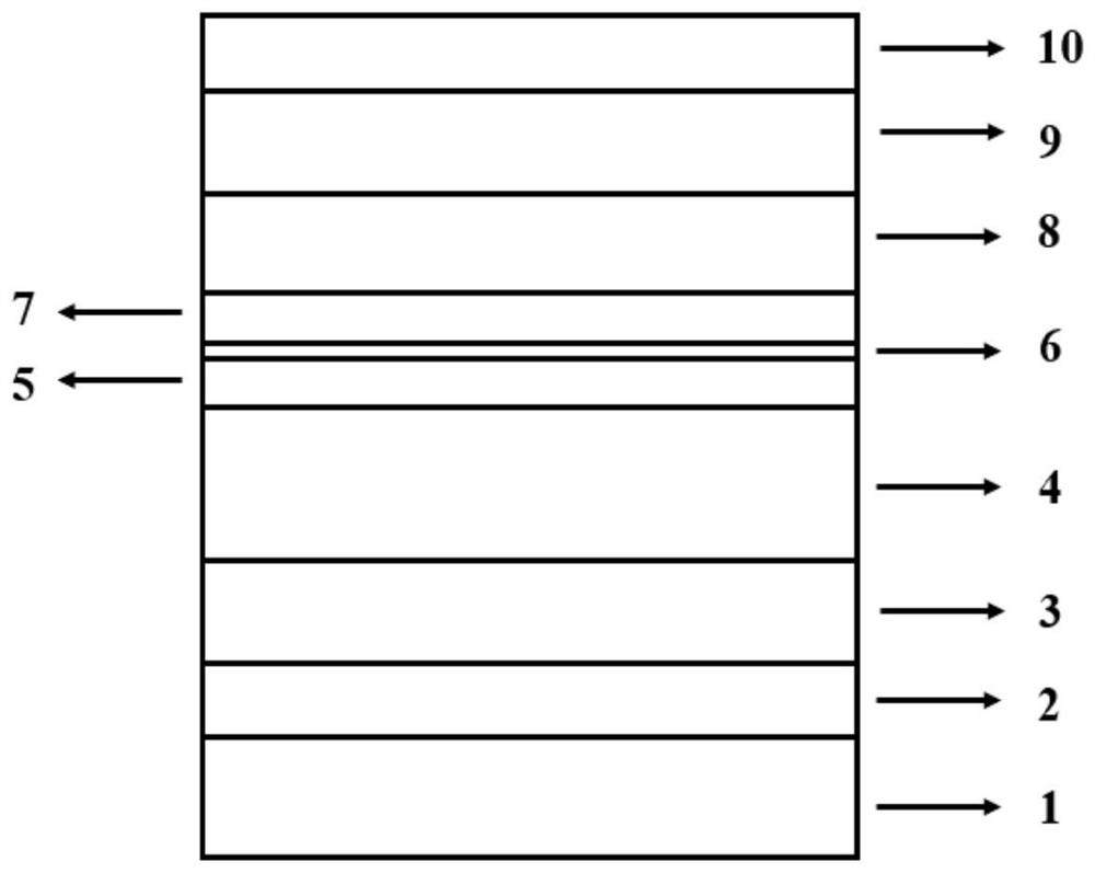
[0034] In this embodiment, a semiconductor laser structure is specifically disclosed, aiming to solve the problems of low fundamental mode confinement factor and high gain of high-order mode modes in the existing large optical cavity waveguide structure 790nm semiconductor laser, such as figure 1 As shown, the structure includes:

[0035] The substrate 1, the buffer layer 2, the lower confinement layer 3, the lower waveguide layer 4, the active layer 6, the upper waveguide layer 8, the upper confinement layer 9 and the ohmic contact layer 10 are arranged respectively from bottom to top, wherein, in the High refractive index layers are respectively embedded between the lower waveguide layer 4 and the active layer 6 and between the active layer 6 and the upper waveguide layer 8, and the active layer 6 is also called a quantum well. The advantage of this design method is that a high refractive index layer is embedded between the active layer 6 and the waveguide layers on both sid...

Embodiment 2

[0056] On the basis of Embodiment 1, in this embodiment, the high refractive index layer, substrate 1, buffer layer 2, lower confinement layer 3, lower waveguide layer 4, active layer 6, upper waveguide layer 8, upper confinement layer Layer 9 and ohmic contact layer 10 are selected as follows:

[0057] ① High refractive index layer

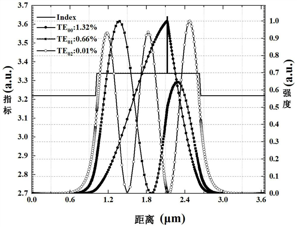
[0058] A high refractive index layer between the upper waveguide layer 8 and the active layer 6, which is unintentionally doped In 0.49 Ga 0.51 As 0.1 P 0.9 material and a thickness of 10 nm; a high refractive index layer between the lower waveguide layer 4 and the active layer 6, which is unintentionally doped In 0.49 Ga 0.51 As 0.1 P 0.9 material and a thickness of 10 nm. Since In 0.49 Ga 0.51 As 0.1 P 0.9 The material layer does not contain Al components, and there is no phenomenon of catastrophic optical damage to the cavity surface easily caused by the oxidation of Al components on the cavity surface;

[0059] The high refractiv...

Embodiment 3

[0073] On the basis of Embodiment 1, in this embodiment, the high refractive index layer, substrate 1, buffer layer 2, lower confinement layer 3, lower waveguide layer 4, active layer 6, upper waveguide layer 8, upper confinement layer Layer 9 and ohmic contact layer 10 are selected as follows:

[0074] ① High refractive index layer

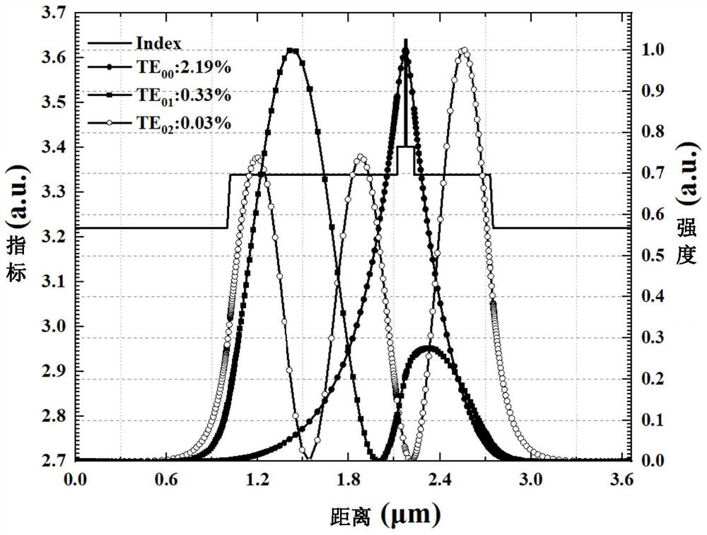
[0075] A high refractive index layer between the upper waveguide layer 8 and the active layer 6, which is unintentionally doped In 0.1 Ga 0.9 As 0.5 P 0.5 material and a thickness of 100 nm; a high refractive index layer between the lower waveguide layer 4 and the active layer 6, which is unintentionally doped In 0.1 Ga 0.9 As 0.5 P 0.5 material and a thickness of 100 nm. Since In 0.1 Ga 0.9 As 0.5 P 0.5 The material layer does not contain Al components, and there is no phenomenon that catastrophic light damage to the cavity surface is easily caused by the oxidation of the Al components on the cavity surface.

[0076] The high refrac...


PUM

PropertyMeasurementUnit
thicknessaaaaaaaaaa
thicknessaaaaaaaaaa
thicknessaaaaaaaaaa

Abstract

The invention discloses a semiconductor laser structure, which belongs to the technical field of semiconductor optoelectronics. The structure includes: a substrate, a buffer layer, a lower confinement layer, a lower waveguide layer, an active layer, an upper waveguide layer, and The upper confinement layer and the ohmic contact layer, wherein high refractive index layers are respectively embedded between the lower waveguide layer and the active layer, and between the active layer and the upper waveguide layer, so as to effectively improve the performance of the large optical cavity waveguide structure. Fundamental mode confinement factor, while enhancing the confinement of the waveguide to the carrier, reducing the threshold current of the device, reducing the mode gain of the high-order mode, thereby increasing the fundamental mode output power of the semiconductor laser with a large optical cavity waveguide structure, improving the beam quality, and preparing high-performance The 790nm high power semiconductor laser lays the foundation for the purpose.

Description

technical field [0001] The invention belongs to the technical field of semiconductor optoelectronics, and in particular relates to a semiconductor laser structure. Background technique [0002] High-power semiconductor lasers are widely used in civil and military fields such as medical treatment, mechanical processing, communication, guidance, pumping solid-state lasers and fiber lasers. Among them, semiconductor lasers with a wavelength near 790nm are mainly used for pumping thulium (Tm) fiber lasers and for laser beauty, material processing, and physical therapy. The market demand is large, but the performance requirements for lasers are relatively high. At present, most domestic manufacturers can only produce small and medium power semiconductor lasers in the 790nm band. Only a few companies in Germany, the United States and other countries can produce high-power 790nm semiconductor lasers, and because some products such as laser arrays can be used in military affairs, t...

Claims


Application Information

Patent Timeline
Patent Type & Authority Patents(China)
IPC IPC(8): H01S5/20H01S5/30
CPCH01S5/2027H01S5/3013
Inventor 何林安周坤杜维川李弋高松信唐淳
Owner INST OF APPLIED ELECTRONICS CHINA ACAD OF ENG PHYSICS
Why Eureka
Try Eureka