High-efficiency semiconductor laser

A laser and semiconductor technology, applied in the structure of optical waveguide semiconductors, etc., can solve the problems of high power density, reduced electro-optical conversion efficiency, uneven distribution of optical power density, etc., and achieve the effect of improving efficiency

Pending Publication Date: 2022-01-18
INST OF APPLIED ELECTRONICS CHINA ACAD OF ENG PHYSICS
View PDF6 Cites 0 Cited by
  • Summary
  • Abstract
  • Description
  • Claims
  • Application Information

AI Technical Summary

Problems solved by technology

However, the asymmetry of the reflectivity of the front and rear cavity surfaces causes the optical power density distribution along the resonant cavity inside the chip to be severely uneven, and the closer to the front cavity, the higher the power density.
The current density inside the chip is generally uniform along the direction of the resonant cavity, which causes the spatial hole burning effect, resulting in less carrier consumption and more remaining carriers in the area close to the rear cavity of the chip, and the current leaks, spontaneously radiates or non-conductively. Radiative recombination in the form of recombination, thereby reducing the efficiency of electro-optical conversion

Method used


Image

  • High-efficiency semiconductor laser
  • High-efficiency semiconductor laser

Examples


Embodiment 1

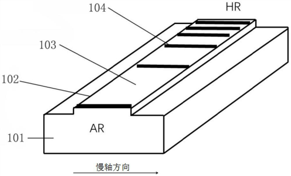
[0027] Aiming at the problem of the spatial hole burning effect in the current bar-type semiconductor laser, a high-efficiency semiconductor laser is specifically provided in this embodiment, such as figure 1 As shown, it mainly includes a substrate 101 .

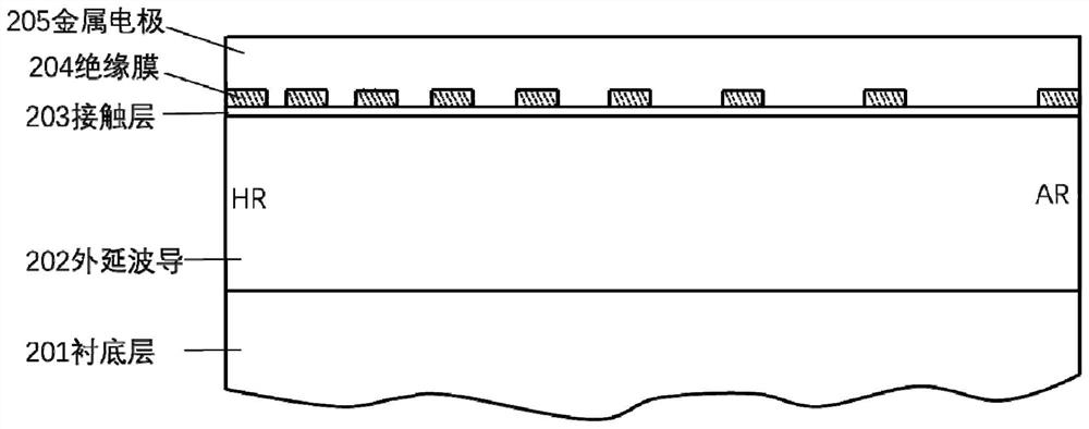
[0028] Also includes: a strip waveguide 102 arranged on the substrate 101, the strip waveguide 102 is arranged on the substrate 101, the width of the strip waveguide 102 is 100 microns, the etching depth of the strip waveguide 102 is 500nm, the strip waveguide 102 has a length of 4 mm. Such as figure 2 As shown, the strip waveguide 102 includes an epitaxial waveguide 202 disposed on the upper side of the substrate 101 layer, the upper side of the epitaxial waveguide 202 is provided with a contact layer 203, and the upper side of the contact layer 203 is arranged with the insulating regions at intervals. 104 , and the upper side of the contact layer 203 is covered with a metal electrode 205 . Wherein, each insulating reg...

Embodiment 2

[0034] Aiming at the problem of the spatial hole-burning effect in the current bar-type semiconductor laser, another high-efficiency semiconductor laser is specifically provided in this embodiment, and its structure is shown in figure 1 , figure 2 shown. During implementation of this embodiment, a strip waveguide 102 is provided on the substrate 101. The width of the strip waveguide 102 is 120 microns, the etching depth of the strip waveguide 102 is 550 nm, and the length of the strip waveguide 102 is 5 mm. Such as figure 2 As shown, the strip waveguide 102 includes an epitaxial waveguide 202 disposed on the upper side of the substrate 101 layer, the upper side of the epitaxial waveguide 202 is provided with a contact layer 203, and the upper side of the contact layer 203 is arranged with the insulating regions at intervals. 104 , and the upper side of the contact layer 203 is covered with a metal electrode 205 . Wherein, each insulating region 104 is an insulating film 2...


PUM

PropertyMeasurementUnit
depthaaaaaaaaaa
reflectanceaaaaaaaaaa

Abstract

The invention discloses a high-efficiency semiconductor laser, and belongs to the technical field of semiconductor laser devices. The laser comprises a substrate and a strip-shaped waveguide arranged on the substrate, a plurality of insulating regions are arranged on the strip-shaped waveguide along the direction of a resonant cavity, the strip-shaped waveguide is divided into a plurality of electric injection regions by the insulating regions, and the interval between every two adjacent insulating regions is gradually increased from the rear cavity surface to the front cavity surface of the laser, so that the purposes of inhibiting space hole burning in the strip-type semiconductor laser and improving the electro-optical conversion efficiency are achieved.

Description

technical field [0001] The invention belongs to the technical field of semiconductor laser devices, and in particular relates to a high-efficiency semiconductor laser. Background technique [0002] Semiconductor lasers are widely used in pumping solid-state and fiber lasers, material processing, and laser medical treatment due to their advantages such as compact structure, low cost, and easy control of the optical field. Among them, the strip-type semiconductor laser has a simple manufacturing process and high electro-optical efficiency, and is the main device structure used in high-efficiency semiconductor lasers. [0003] Usually, bar-type semiconductor lasers need to vapor-deposit AR high-transmittance film on the front cavity surface, and evaporate HR high-reflectivity film on the rear cavity surface, so that the laser can output from the front cavity surface. However, the asymmetry of the reflectivity of the front and rear cavity surfaces causes the optical power densi...

Claims


Application Information

Patent Timeline
Patent Type & Authority Applications(China)
IPC IPC(8): H01S5/22
CPCH01S5/22
Inventor 周坤杜维川何林安贺钰雯李弋高松信唐淳张亮胡耀杨鑫
Owner INST OF APPLIED ELECTRONICS CHINA ACAD OF ENG PHYSICS
Why Eureka
Try Eureka