Sub-pixel circuit, active electroluminescence display and driving method thereof

A technology of electroluminescence and pixel circuits, applied to static indicators, instruments, etc., can solve the problems of signal switching delay and limit the development of high-resolution drive, etc., to increase the number of gray scales, improve the time of signal switching, and improve The effect of resolution

Active Publication Date: 2021-03-23
CHONGQING KONKA PHOTOELECTRIC TECH RES INST CO LTD
View PDF7 Cites 0 Cited by
  • Summary
  • Abstract
  • Description
  • Claims
  • Application Information

AI Technical Summary

Problems solved by technology

However, under ideal conditions, the signal waveform in the circuit line is as shown in the ideal waveform (1), but the actual waveform after power-on is as shown in the actual waveform (2). Furthermore, when a large current is directly introduced into the chip, the rise of the actual waveform is slower than that of the chip. Ideal waveform, it will cause the problem of signal switching delay, thus limiting the development of high-resolution drive

Method used


Image

  • Sub-pixel circuit, active electroluminescence display and driving method thereof
  • Sub-pixel circuit, active electroluminescence display and driving method thereof
  • Sub-pixel circuit, active electroluminescence display and driving method thereof

Examples


Embodiment Construction

[0042] The present invention provides a sub-pixel circuit, an active electroluminescence display and a driving method thereof. PWM driving is applied to an AM (Active Matrix / active matrix) panel structure, which can effectively reduce the driving load and split the sub-pixel Multiple signal lines, thereby greatly improving the resolution.

[0043] In order to make the object, technical solution and effect of the present invention more clear and definite, the present invention will be further described in detail below with reference to the accompanying drawings and examples. It should be understood that the specific embodiments described here are only used to explain the present invention, not to limit the present invention.

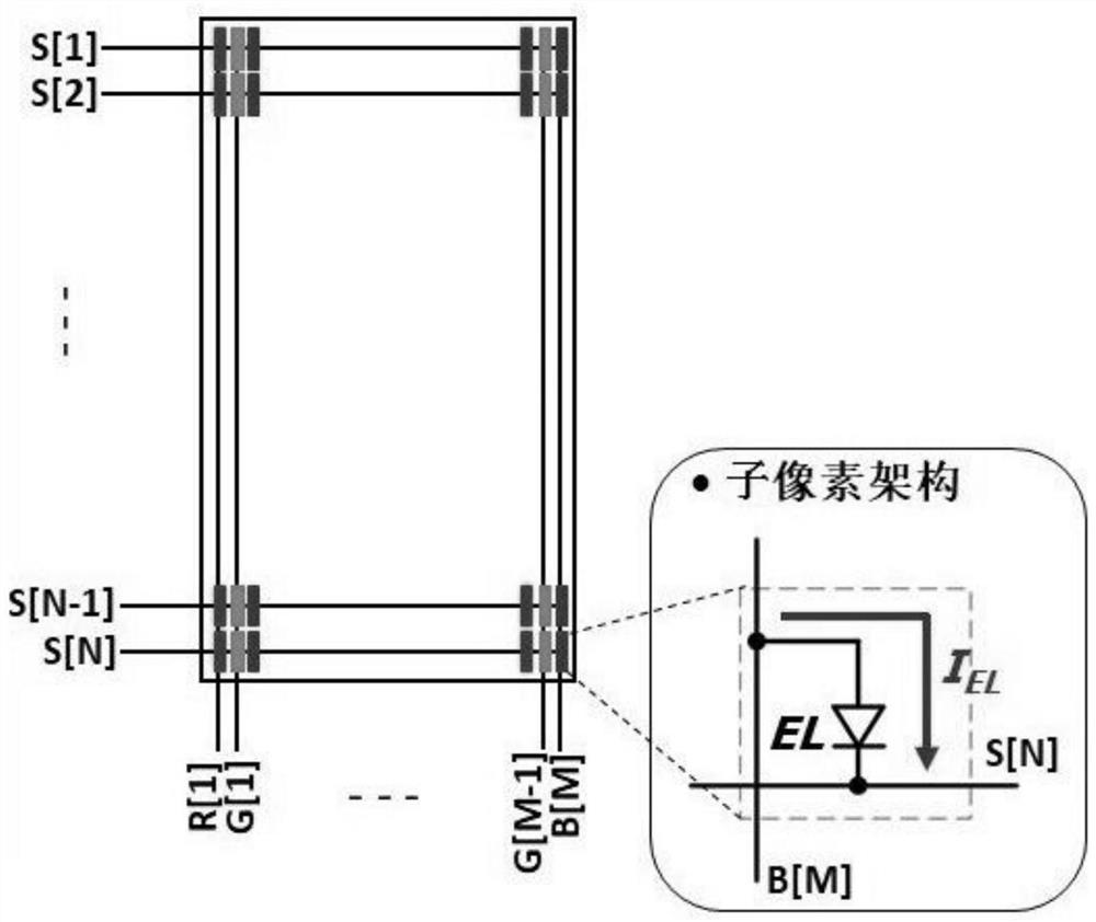
[0044] see image 3 , Figure 4 with Figure 5 , the sub-pixel circuit provided by the present invention includes at least one electroluminescence device and a first drive transistor Q1 or a second drive transistor Q2 and a third drive transistor Q3 co...


PUM


Abstract

The invention discloses a sub-pixel circuit, an active electroluminescence display and a driving method thereof. The sub-pixel circuit includes at least one electroluminescence device and a first drive transistor or a second drive transistor connected to the electroluminescence device. and the third driving transistor; the cathode of the electroluminescent device is connected to electricity, the anode of the electroluminescent device is connected to the output terminal of the first driving transistor, and the input terminal of the first driving transistor is connected to the signal line, so The control end of the first drive transistor is connected to the scan line; or the anode of the electroluminescence device is connected to the output end of the second drive transistor, the input end of the second drive transistor is connected to the output end of the third drive transistor, and the third drive transistor is connected to the output end of the third drive transistor. The input end of the drive transistor is connected to electricity, the control end of the second drive transistor is connected to the scan line, and the control end of the third drive transistor is connected to the signal line. By reducing the load on the scan line and the signal line and changing the number of signal lines, the resolution is improved. Rate.

Description

technical field [0001] The invention relates to the field of display technology, in particular to a sub-pixel circuit, an active electroluminescence display and a driving method thereof. Background technique [0002] EL (Electroluminescence / Electroluminescence) devices, including: OLED (Organic Light-Emitting Diode, OLED / Organic Light Emitting Diode), LED (Light Emitting Diode, LED / Light Emitting Diode)... etc., have been widely used in the production of display products in recent years, Compared with traditional displays (CRT, LCD, etc.), its application surface shows better optical characteristics, lower power consumption performance, better product shape plasticity, and PWM (Pulse Width Modulation / pulse width adjustment method ) drive is one of the methods widely used to control EL displays. The luminance and gray scale are determined by adjusting the luminous time, and it provides a solution for the brightness linearity of the display. [0003] The traditional PWM drivi...

Claims


Application Information

Patent Timeline
Patent Type & Authority Patents(China)
IPC IPC(8): G09G3/32G09G3/3216G09G3/3225
CPCG09G3/32G09G3/3216G09G3/3225G09G2320/0223G09G3/2014G09G2300/0809G09G2300/08G09G3/3258G09G2320/0252G09G2310/0202G09G2330/02G09G3/3208
Inventor 郑士嵩
Owner CHONGQING KONKA PHOTOELECTRIC TECH RES INST CO LTD
Why Eureka
Try Eureka