Supercharge Your Innovation With Domain-Expert AI Agents!

Power device embedded substrate packaging structure and preparation method

A power device and packaging structure technology, applied in the field of power device embedded substrate packaging structure and preparation, can solve the problems of undrilled holes, floating pads, Al melting of pads, etc., to improve processing yield, Effect of Reliability Improvement

Pending Publication Date: 2020-06-26
SHANGHAI FINE CHIP SEMICON
View PDF9 Cites 0 Cited by
  • Summary
  • Abstract
  • Description
  • Claims
  • Application Information

AI Technical Summary

Problems solved by technology

Usually, the material of the upper electrode pad of the chip is a thin metal Al layer. If the hole is drilled directly on the thin metal Al layer, if the energy is too large, it will cause the pad to float away, and more seriously, it will cause the pad to be damaged. Al is melted; but if the energy is too small, holes will not be drilled
Therefore, it is necessary to increase the thickness of the electrode pad metal layer on the chip to increase the process redundancy of laser drilling, but if the thickness of the pad metal Al layer is simply increased, it will bring great processing difficulty to the entire front-end process

Method used


Image

  • Power device embedded substrate packaging structure and preparation method
  • Power device embedded substrate packaging structure and preparation method
  • Power device embedded substrate packaging structure and preparation method

Examples


Embodiment 1

[0051] A method for preparing a power device embedded substrate packaging structure, comprising the following steps:

[0052] Step 1: Preparation of Power Semiconductor Die

[0053] 1.1 see Figure 5 , the upper surface of the silicon layer 110 is covered with a dielectric layer 130, a passivation layer 140, and a bonding pad Al layer 111, a part of the bonding pad Al layer 111 is directly connected to the silicon layer 110, and another part of the bonding pad Al layer 111 A dielectric layer 130 is provided between a part and the silicon layer 110, and the adjacent pad Al layers 111 are separated by a passivation layer 140;

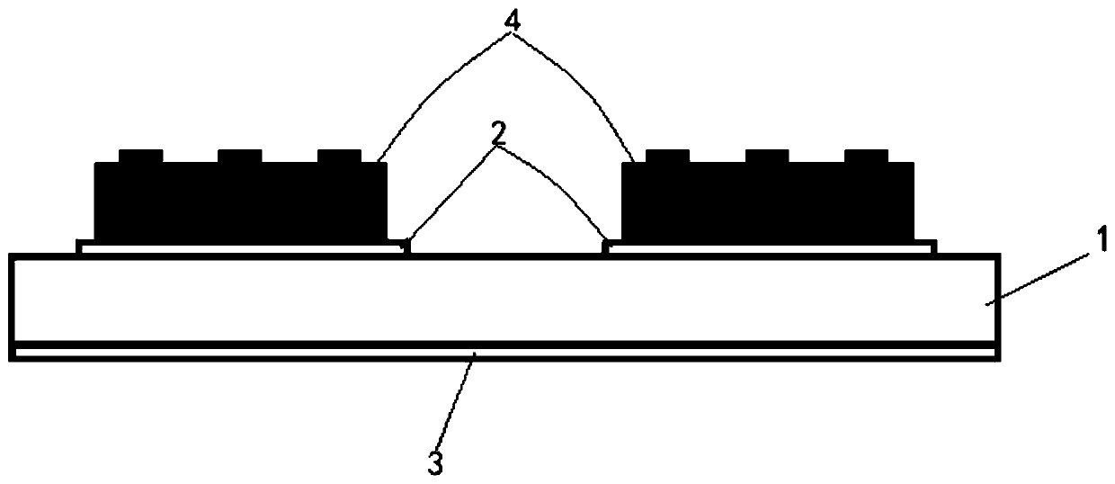
[0054] 1.2 see Image 6 , make conductive column 112 on each pressure pad Al layer 111 to form the upper electrode 110 of the power semiconductor die; conductive column 112 can be nickel column, copper column or gold column or other metal materials, nickel column can adopt electroless plating The metal nickel is formed, the copper pillar can be formed ...

Embodiment 2

[0066] Steps 1 and 2 of the method for preparing a power device embedded substrate packaging structure in this embodiment are the same as those in Embodiment 1, except that Step 3.2 and Step 3.3 in Step 3 are different, see Figure 14 , Step 3 of this embodiment is replaced by the following steps 3.2a and 3.3a:

[0067] 3.2a Use flow glue 300 to fill each power semiconductor die A and cover each power semiconductor die A for dielectric lamination, then directly grind the upper surface of flow glue 300, and place the upper electrode in each power semiconductor die A The upper surface of the conductive pillar 112 of 110 exposes the upper surface of the flow glue 300 to form a laminated substrate embedded with power semiconductor dies;

[0068] 3.3a ​​Use a laser to punch some blind holes 320 and some through holes 330 on the substrate embedded with the power semiconductor die after lamination, and the blind holes 320 expose the lower electrode 120 of the power semiconductor die ...


PUM


Abstract

The invention discloses a power device embedded substrate packaging structure which is characterized by comprising a power semiconductor tube core and a substrate, wherein the power semiconductor tubecore is laminated on the substrate through a gummosis layer, and a plurality of blind holes and a plurality of through holes are formed in the gummosis and are metalized, so that the electrodes of the power semiconductor tube core are connected with an outer-layer circuit copper foil; after graphical processing is carried out on the outer layer circuit copper foil, ball mounting and cutting are carried out to form the power device embedded substrate packaging structure. The invention further discloses a preparation method of the device-embedded substrate packaging structure. According to thepresent invention, the technical problems existing in the prior art are solved; the laser trepanning is carried out on a conductive column of the upper electrode in the power semiconductor tube core,so that the processing redundancy is much greater than that of a previous bonding pad Al layer, and the processing yield can be greatly improved; in addition, the bonding pad Al layer is well connected with the conductive columns, so that the reliability is improved.

Description

technical field [0001] The invention relates to the technical field of embedded substrate packaging, in particular to a power device embedded substrate packaging structure and a preparation method. Background technique [0002] With the rapid increase of light, thin, high-performance portable electronic devices, a new type of substrate-level packaging technology that embeds electronic components inside the substrate has emerged in large numbers. Embedded packaging technology not only embeds passive components in the substrate, but also embeds active devices in the organic substrate. This packaging technology can not only shorten the leads between active and passive devices and improve the overall performance, but also is extremely beneficial to realize ultra-small and thin. [0003] In order to achieve this goal, it is obviously impossible to use high-temperature sintering of ceramics. The only effective and feasible way is to use organic substrates, and IC components, unli...

Claims


Application Information

Patent Timeline
Patent Type & Authority Applications(China)
IPC IPC(8): H01L23/498H01L23/31H01L21/48H01L21/56H01L21/60
CPCH01L23/49816H01L23/49838H01L23/49811H01L23/3114H01L23/3128H01L21/56H01L21/4853H01L24/81H01L2224/81009H01L2224/18
Inventor 黄平鲍利华顾海颖
Owner SHANGHAI FINE CHIP SEMICON
Features
  • R&D
  • Intellectual Property
  • Life Sciences
  • Materials
  • Tech Scout
  • Unparalleled Data Quality
  • Higher Quality Content
  • 60% Fewer Hallucinations
Learn More