
Distributed SRAM failure analysis method and system

A failure analysis and distributed technology, applied in special data processing applications, instruments, electrical digital data processing, etc., can solve the problems of inconvenient analysis and long analysis time, reduce reading time, improve rendering efficiency, and reduce transmission load Effect

Active Publication Date: 2020-07-03
SEMITRONIX
View PDF7 Cites 1 Cited by
  • Summary
  • Abstract
  • Description
  • Claims
  • Application Information

AI Technical Summary

Problems solved by technology

The analysis time is too long, which greatly restricts the engineers to discover the problems in the manufacturing in time
In addition, since there are about 1 billion pixels on a wafer, the current rendering technology requires the user to wait for a few minutes, which also brings a lot of inconvenience to the engineer's analysis

Method used


Image

  • Distributed SRAM failure analysis method and system
  • Distributed SRAM failure analysis method and system
  • Distributed SRAM failure analysis method and system

Examples


Embodiment 1

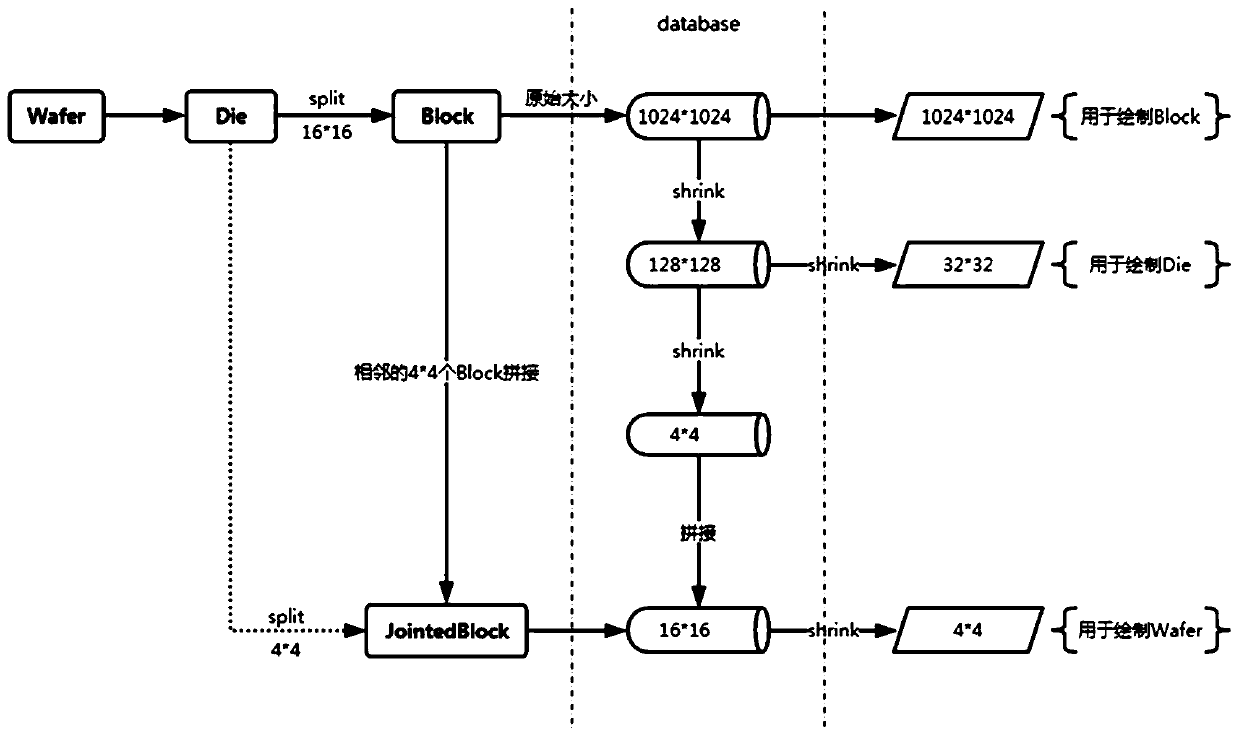
[0061] use figure 1 The SRAM data of the process shown in the detailed description of the data compression method used for distributed SRAM failure analysis:

[0062] 1) Compressed storage:

[0063] The database stores data at the Block level, data at the Die level, and data at the Wafer level.

[0064] After decoding the data at the block level, the resolution of each block is 1024×1024; after decoding the data at the Die level, the resolution of each block is 128×128; after decoding the data at the Wafer level, the resolution of each block is 16×16.

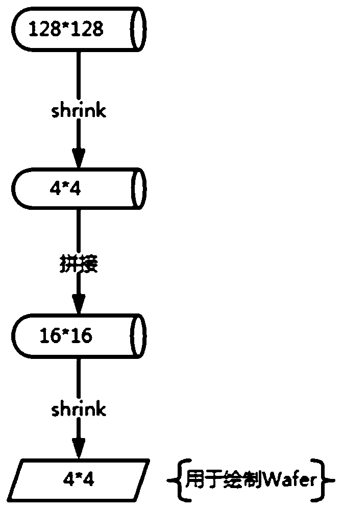
[0065] For the splicing processing of the sampled data during sampling, please refer to figure 1 The data compression process at the middle Wafer level: sampling the analysis result data to compress the resolution of each block to 4×4, and then stitching adjacent 4×4 blocks to obtain a Jointed Block, so that each Block( The resolution of Jointed Block is 16×16.

[0066] 2) Sampling and drawing:

[0067] When drawing a block, directly pr...

Embodiment 2

[0070] Example 2 SRAM test

[0071] According to the definition of the original Block: each Die contains 16×16 Blocks, each Block 1024×1024; at the Wafer level, if a wafer has 84 Dies, the number of Block records contained reaches: 84×256×14 =301056. The 14 multiplied here refers to the test voltage Voltage.

[0072] When dividing tasks for each thread, you need to get all the corresponding Fail Types. At the Die level, only 3584 records need to be traversed. At the Wafer level, the number reaches 301056, which leads to taking this part of the data. Time-consuming has increased significantly. According to the actual measurement, it takes 1500ms to obtain all Fail Types at the first level of Wafer, which accounts for more than 70% of the total background processing time.

[0073] At the wafer level, the original 16 (4×4) blocks (the original resolution is 1024×1024, compressed to 4×4 when stored) are spliced ​​together to obtain a new Jointed Block with a resolution of 16 ×16, the...

Embodiment 3

[0099] Example 3 Simulation and simulation of storage space

[0100] Storage space estimation: A block requires up to 128K of storage space, and a die is 32MB. On the basis of binary coding, the binary data is compressed, which can further reduce the storage space of each die. After the data analysis is completed, a die may have more than 10 types of failures, and the uncompressed storage space will be 10*32M, but the analysis result data is relatively sparse and exhibits more obvious distribution characteristics, so after compression, the space station occupied less than This value. According to actual experiments, regardless of the distribution characteristics of the analysis results, the compressed storage space will not exceed 2*32M. According to the actual simulation, the space occupied by the test data we constructed will increase significantly when the failure rate is 50%. The raw data and analysis data of a die occupy about 33MB, and when the failure rate is less than 4...


PUM


Abstract

The invention relates to a distributed SRAM failure analysis method and system. The distributed SRAM (Static Random Access Memory) failure analysis method comprises the following steps of: A, acquiring an SRAM test data result as original data and performing failure analysis on the original data to obtain failure analysis result data; b, performing binary coding compression on the analysis resultdata according to a preset binary coding rule, and injecting the compressed analysis result data into a distributed database; and C, extracting analysis result data to be displayed from the distributed database, decoding the extracted data according to a preset binary decoding rule, sampling the decoded analysis result data according to a preset data sampling rule according to a resolution requirement during drawing, and drawing and displaying the data at the front end. According to the method, the original occupied space of one wafer can be effectively compressed, and the SRAM failure analysis efficiency is improved.

Description

Technical field [0001] The invention relates to the field of semiconductor design and production, and particularly relates to a distributed SRAM failure analysis method and system. Background technique [0002] SRAM is widely used by most wafer foundries for process debugging of newly introduced processes and process monitoring that has been put into actual use. Using the addressability of SRAM, it is easier to locate the failure point, and confirm it through physical failure analysis methods such as atomic force microscope probe (AFP), scanning electron microscope (SEM), etc., analyze the cause of the failure, and locate the failure. Process steps and make improvements. [0003] With the continuous improvement of chip integration, the feature size of integrated circuits continues to shrink at an exponential rate. Static Random Access Memories (Static Random Access Memories) testing and failure analysis occupy an increasingly important position. On the one hand, due to its high-...

Claims


Application Information

Patent Timeline
Patent Type & Authority Applications(China)
IPC IPC(8): G06F30/398
Inventor 邵康鹏陆梅君杨慎知
Owner SEMITRONIX
Learn More