Special protection circuit in silicon carbide diode chip

A technology of silicon carbide diodes and protection circuits, applied in emergency protection circuit devices, emergency protection circuit devices for limiting overcurrent/overvoltage, circuits, etc., can solve the problem of increasing the complexity of the structure of the protection circuit, potential safety hazards, There are problems such as electromagnetic interference to achieve the effect of avoiding high voltage breakdown, improving protection performance, and preventing electromagnetic interference

Inactive Publication Date: 2020-07-10
CHANGZHOU GIANTION PHOTOELECTRICITY IND DEV
View PDF4 Cites 2 Cited by
  • Summary
  • Abstract
  • Description
  • Claims
  • Application Information

AI Technical Summary

Problems solved by technology

The protection circuits of these two settings require long lead wires, and there is electromagnetic interference; the external protection circuit increases the complexity of the structure, and there are potential safety hazards

Method used


Image

  • Special protection circuit in silicon carbide diode chip
  • Special protection circuit in silicon carbide diode chip
  • Special protection circuit in silicon carbide diode chip

Examples


Embodiment 1

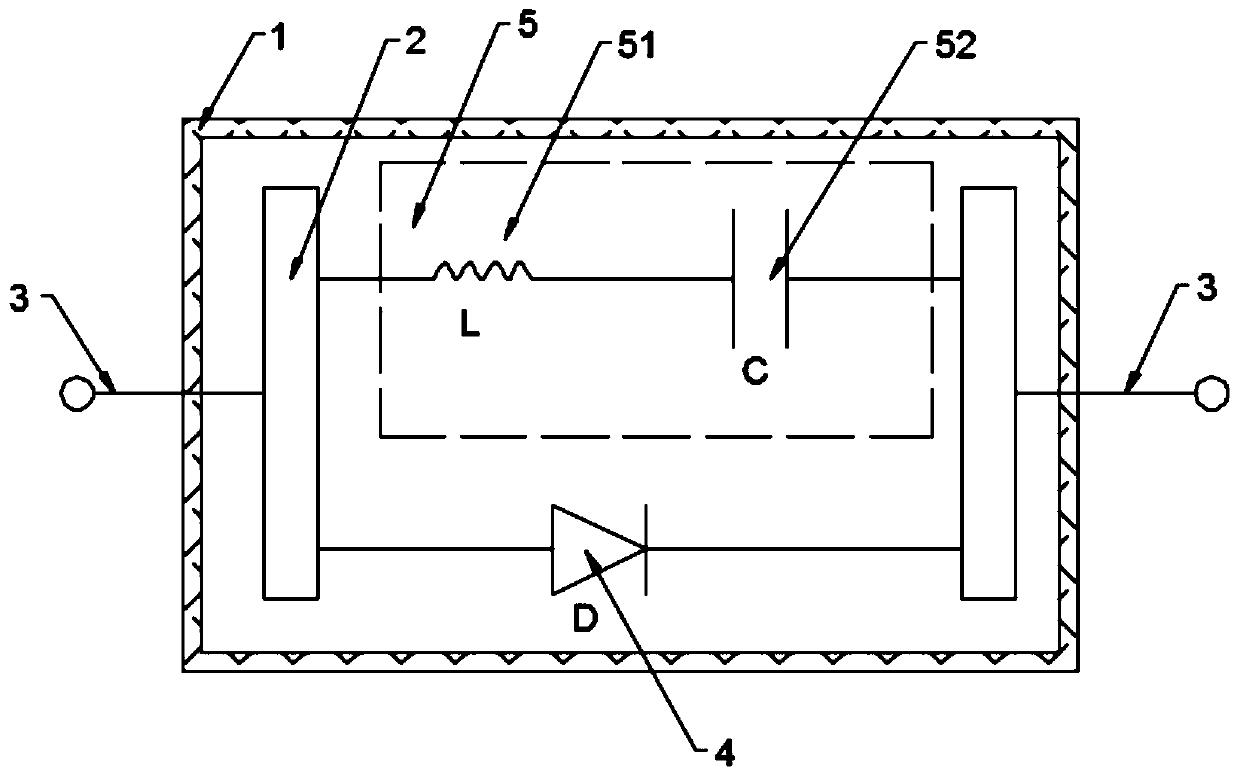
[0024] refer to figure 1 , a dedicated protection circuit in a silicon carbide diode chip, including a package shell (1), a group of chips 2 located in the package shell 1, and leads 3 connected to both ends of the package shell 1, and the package shell 1 is made of black glue , the chip is provided with a silicon carbide diode 4 and a protection circuit 5, the protection circuit 5 includes an inductance 51 and a capacitor 52, and the protection circuit 5 formed by the inductance 51 and the capacitor 52 in series is connected in parallel with the silicon carbide diode 4; Due to the influence of space size and heat dissipation performance, the capacitor 52 and the resistor 53 are sheet or printed structures; the inductor 51 can be a separate lead inductor, or a serpentine lead that is depicted and printed on the chip.

Embodiment 2

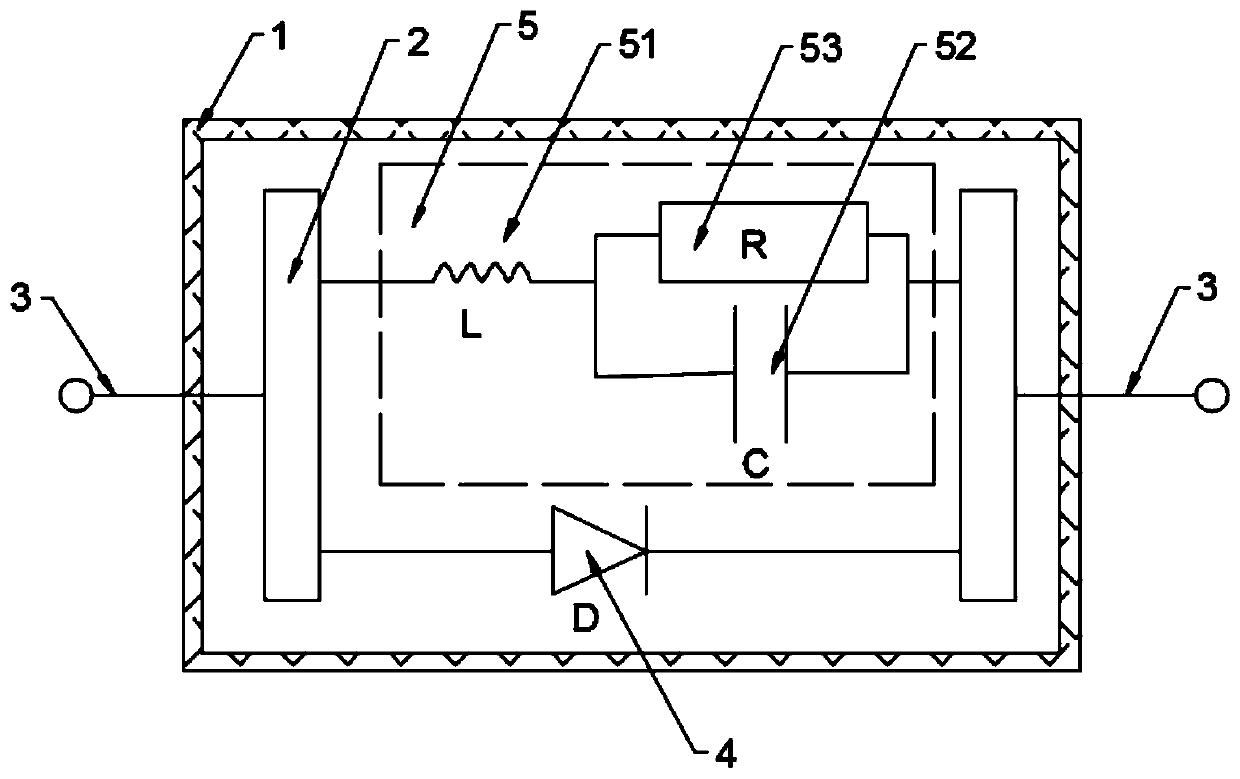
[0026] refer to figure 2 , a special protection circuit in the silicon carbide diode chip, including a package shell 1, a group of chips 2 located in the package shell 1, and leads 3 connected to both ends of the package shell 1. The package shell 1 is made of black glue, and the said package shell 1 is made of black glue. The chip is provided with a silicon carbide diode 4 and a protection circuit 5. The protection circuit 5 includes an inductor 51, a capacitor 52 and a resistor 53. The resistor 53 is connected in parallel with the capacitor 52, and then connected in series with the inductor 51; the protection circuit 5 is connected to the silicon carbide. The diode 4 is connected in parallel; the capacitor 52 and the resistor 53 are sheet or printed structures according to the influence of the internal space and heat dissipation performance; the inductor 51 can be a separate lead inductor, or a serpentine lead drawn and printed on the chip.

[0027] This embodiment and the ...

Embodiment 3

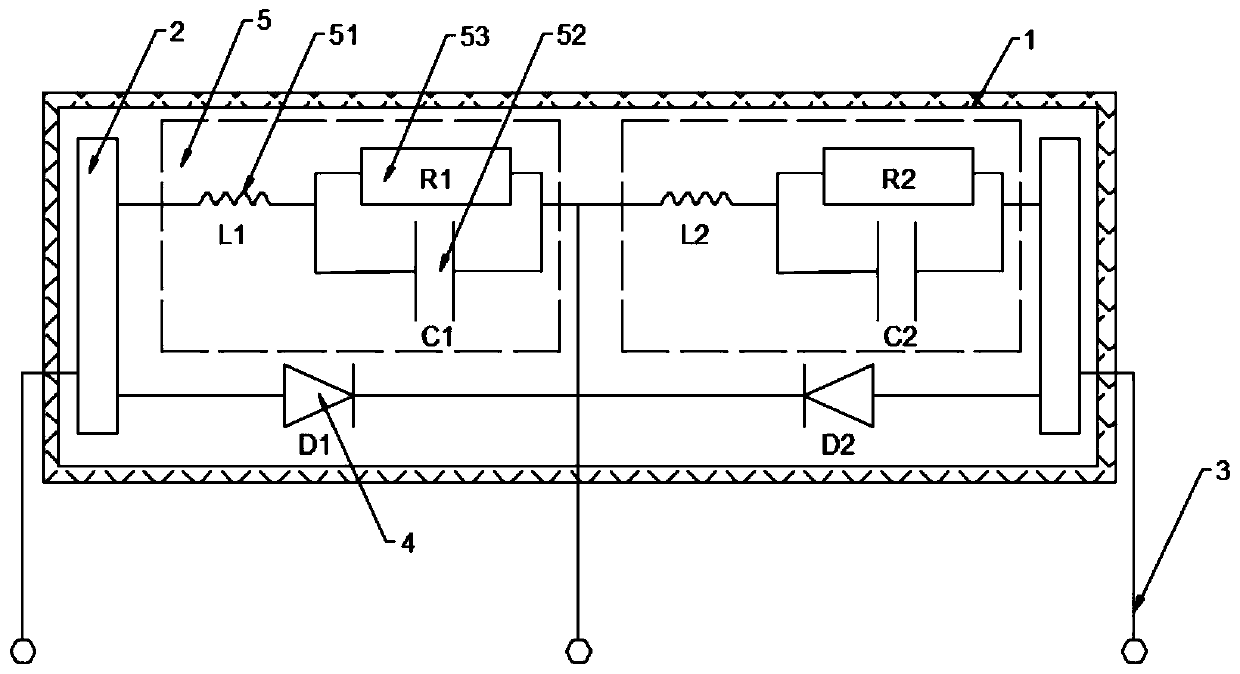
[0029] refer to image 3 , a special protection circuit in the silicon carbide diode chip, including a package shell 1, a group of chips 2 located in the package shell 1, and leads 3 connected to both ends of the package shell 1, and the package shell 1 is made of black glue; the said package shell 1 is made of black glue; There is a common cathode in the chip and two silicon carbide diodes 4 are arranged in parallel. Each silicon carbide diode 4 is connected in parallel with a protection circuit 5. The protection circuit 5 includes an inductor 51, a capacitor 52 and a resistor 53. The resistor 53 is connected to the capacitor. 52 is connected in parallel, and then connected in series with the inductor 51; the protection circuit 5 is connected in parallel with the silicon carbide diode 4; specifically: the silicon carbide diode 4 includes a silicon carbide diode D1 and a silicon carbide diode D2, and the silicon carbide diode D1 is connected with the inductor L1, the capacitor ...


PUM


Abstract

The invention belongs to the technical field of semiconductors. The invention relates to a special protection circuit in a silicon carbide diode chip. The special protection circuit comprises a packaging shell, one or more chips which are located in the packaging shell and connected in series, and leads which are connected to the two ends of the packaging shell, a silicon carbide diode and a protection circuit are arranged in each chip, the protection circuit comprises an inductor and a capacitor, and the protection circuit formed by connecting the inductor and the capacitor in series is connected with the silicon carbide diode in parallel; the protection circuit further comprises a resistor connected with the capacitor in parallel, and the capacitor and the resistor which are connected inparallel are connected with the inductor in series. The special protection circuit eliminates and absorbs peak high voltage and high-frequency interference harmonic waves generated by the silicon carbide diode and an inductance element during application in a packaging structure, so that the circuit is protected, and the service life of the silicon carbide diode is prolonged; the width of the forbidden band is stabilized and widened, the depth is increased, and parasitic harmonics are absorbed.

Description

technical field [0001] The invention belongs to the technical field of semiconductors, and in particular relates to a dedicated protection circuit in a silicon carbide diode chip. Background technique [0002] Silicon carbide is the most mature wide-bandgap semiconductor material at present. Compared with ordinary silicon components, it has high withstand voltage and is widely used in switching power supplies and high-frequency rectifiers. However, due to its application in high-voltage circuits, when there is a reverse electromotive force, there are dangers such as creepage and leakage, and there are great potential safety hazards; during use, due to the existence of resistance, it will affect the resonant frequency and affect the absorption depth of the diode. . [0003] When the existing silicon diodes are used, due to their limited voltage withstand performance, a safety circuit is usually connected in parallel to protect the circuit; however, when silicon carbide diode...

Claims


Application Information

Patent Timeline
Patent Type & Authority Applications(China)
IPC IPC(8): H02H9/04H01L23/04H01L23/367H05K7/20
CPCH02H9/045H01L23/04H01L23/3675H05K7/2039
Inventor 吕全亚周琦庄娟梅郭建新刘域庭陈莉娜
Owner CHANGZHOU GIANTION PHOTOELECTRICITY IND DEV
Why Eureka
Try Eureka