
Wafer manufacturing process flow of high-performance MEMS inertial sensor

A technique for inertial sensors and capping wafers, applied to the photolithography process of the pattern surface, the process for producing decorative surface effects, manufacturing tools, etc., can solve the complex bonding process and the symmetry error of the output of the accelerometer sensor and other problems, to achieve the effect of simple bonding process, high alignment accuracy and good structural symmetry

Pending Publication Date: 2020-07-17
EAST CHINA INST OF OPTOELECTRONICS INTEGRATEDDEVICE
View PDF4 Cites 0 Cited by
  • Summary
  • Abstract
  • Description
  • Claims
  • Application Information

AI Technical Summary

Problems solved by technology

However, the above process requires the first substrate to etch a deep groove, and then perform pattern alignment bonding, which makes the bonding process complicated; and the thickness of the beam is smaller than the thickness of the proof mass, and the center of gravity of the structure is on the upper side, which will make the accelerometer sensor The output symmetry of ±1G produces a certain error

Method used


Image

  • Wafer manufacturing process flow of high-performance MEMS inertial sensor
  • Wafer manufacturing process flow of high-performance MEMS inertial sensor
  • Wafer manufacturing process flow of high-performance MEMS inertial sensor

Examples


Embodiment

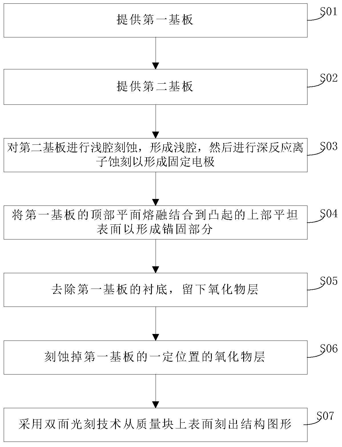
[0052] like figure 1 As shown, the wafer manufacturing process of high-performance MEMS inertial sensors includes the following steps:

[0053] Providing a first substrate S01: providing a first substrate having a top plane and a bottom plane, an oxide layer is disposed below the bottom plane, and the bottom plane is substantially parallel to the top plane; the first substrate is silicon-on-insulator (SOI) , the top silicon thickness is 50-150μm.

[0054] Providing a second substrate S02: providing a second substrate with an upper flat surface; the second substrate is silicon-on-insulator (SOI), and the silicon thickness is about 5-15 μm.

[0055] Shallow cavity etching S03: Perform photolithographic patterning on the second substrate, perform shallow cavity etching, and etch a part of the second substrate from the upper flat surface to a first predetermined depth (3-10 μm) to form a 3-10 μm A shallow cavity, and a plurality of protrusions, each with an upper flat surface, a...


PUM

PropertyMeasurementUnit
thicknessaaaaaaaaaa
thicknessaaaaaaaaaa

Abstract

The invention discloses a wafer manufacturing process flow of an MEMS inertial sensor, which comprises the following steps: providing a first substrate with a top plane and a bottom plane, and arranging an oxide layer below the bottom plane; providing a second substrate having an upper flat surface; etching a portion of the second substrate from the upper flat surface to form a plurality of protrusions and a shallow cavity, each protrusion having an upper flat surface; bonding a top plane of the first substrate to an upper flat surfaces of the protrusions to form an anchoring portion; etchingoff the oxide layer at a certain position of the first substrate; etching a portion of the first substrate from the bottom surface and / or the top surface to a total thickness of the first substrate toform a sensitive structure having a freely rotatable structure. Icon alignment is not needed during silicon-silicon bonding, so that the bonding process is simple, the thickness of the formed beam isequal to that of the mass block, no error is generated, and better structural symmetry is achieved.

Description

technical field [0001] The invention relates to a manufacturing process of an inertial sensor, in particular to a wafer manufacturing method of a MEMS inertial sensor. Background technique [0002] A wide variety of applications, especially aerospace applications such as inertial navigation systems, guidance systems and aeronautical data measurement systems, require high performance accelerometers with near microgravity resolution, high sensitivity, high linearity and low bias drift and gyroscope. The resolution of high-performance accelerometers and gyroscopes is limited by the thermomechanical Brownian noise of the sensor, which is determined by the damping coefficient and mass of the structure and the readout electronics. [0003] Fabrication techniques play a crucial role in ensuring simultaneous access to large mass, large capacitance and small damping, as well as achieving microgravity resolution. Previously, many high-performance silicon accelerometers and gyroscope...

Claims


Application Information

Patent Timeline
Patent Type & Authority Applications(China)
IPC IPC(8): B81C3/00B81C1/00
CPCB81C3/001B81C1/00531B81C1/00349B81B2201/0228
Inventor 郭述文何凯旋刘磊王鹏郭群英
Owner EAST CHINA INST OF OPTOELECTRONICS INTEGRATEDDEVICE
Learn More