Anti-counterfeiting structure based on patterned perovskite single crystal array as well as preparation and application of anti-counterfeiting structure
A patterned, perovskite technology, applied in the field of anti-counterfeiting, can solve problems such as easy forgery of anti-counterfeiting labels, and achieve the effects of avoiding pollution, strong fluorescence intensity, and high quantum yield
- Summary
- Abstract
- Description
- Claims
- Application Information
AI Technical Summary
Problems solved by technology
Method used
Image
Examples
Embodiment 1
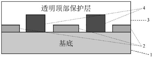
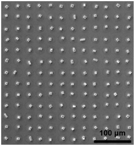
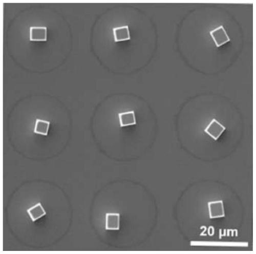
[0055] The anti-counterfeiting structure prepared in this embodiment is as figure 1 As shown, there is a patterned template layer 2 and a perovskite single crystal array 3 on a substrate 1, optionally covered with a transparent top protective layer 4. Among them, the substrate 1 is a glass substrate; the material of the patterned template layer 2 is poly[bis(4-phenyl)(4-butylphenyl)amine] (Poly-TPD), and its pattern is a circular pit with a diameter of 23 μm. The center of the circular pit forms a square lattice, and the distance between the centers of two adjacent circular pits is 30 μm; the material of the perovskite single crystal array 3 is methylamine lead bromine (CH 3 NH 3 PbBr 3 ); the transparent top protective layer 4 is made of polydimethylsiloxane (PDMS).
[0056] The preparation method of the anti-counterfeiting structure based on the patterned perovskite single crystal array of this embodiment specifically includes the following steps:
[0057] 1) Provide the...
Embodiment 2
[0075] In the above embodiments, the patterned perovskite single crystal array is digitally coded using Cartesian coordinates, and digital codes can also be coded by dividing regions. The anti-counterfeit structure and preparation method of the patterned perovskite single crystal array are the same as in the first embodiment. In the part of the anti-counterfeit method, digital coding is carried out by dividing the area code. First, the four vertices of the perovskite single crystal in each pattern pit are coded separately using the method of dividing the area coding, and the direction of the two sides perpendicular to each other of the 3×3 lattice is used as the coordinate axis direction, and each pattern pit The center of the circle is used as the origin of the coordinate axis. For each circular pit, four quadrants are divided, and the numbers from the first quadrant to the fourth quadrant are sequentially recorded as 1 to 4. Each quadrant is divided into equally spaced areas ...
Embodiment 3
[0087] In the above embodiments, no transparent top protective layer is prepared, and the stability of the structure can be improved by adding a transparent top protective layer, and lead leakage can be effectively prevented. The preparation method of the patterned perovskite single crystal array is the same as that of Example 1, and then the polydimethylsiloxane (PDMS) main agent and its curing agent are mixed uniformly at a mass ratio of 10:1 to obtain a PDMS mixed solution. The PDMS mixture was coated on the perovskite single crystal array by doctor blade coating, and then transferred to a vacuum oven at 70°C for 3 hours to form a transparent top protective layer of PDMS.
PUM
| Property | Measurement | Unit |
|---|---|---|
| Linearity | aaaaa | aaaaa |
| Depth | aaaaa | aaaaa |
Abstract
Description
Claims
Application Information


