Method for completing grain cutting of thin wafer by applying plasma grain cutting and laser equipment

A wafer and laser technology, which is applied in the manufacture of circuits, electrical components, semiconductors/solid-state devices, etc., can solve the problem of the inability to apply the double-sided simultaneous metal deposition process of thin wafers and the impossibility of the photoresist spin-coating process of the yellow light process , photoresist failure and other issues

Pending Publication Date: 2020-07-24
绍兴同芯成集成电路有限公司
View PDF6 Cites 1 Cited by
  • Summary
  • Abstract
  • Description
  • Claims
  • Application Information

AI Technical Summary

Problems solved by technology

[0004] 1. The photoresist spin coating process of the yellow light process cannot be carried out, because of its angle structure, the coated photoresist will fail due to the blocking of the edge;
[0005] 2. The proximity yellow light process cannot be applied, because the mask plate of the proximity yellow light process needs to be very close to the wafer, but it is blocked by the frame ring, and the process cannot be carried out in a general and simple way;
[0006] 3. Therefore, the double-sided simultaneous metal deposition process of thin wafers cannot be applied;
[0007] 4. It is placed in the cutting film frame for operation, and it still has ultra-thin wafer cutting, because the cutting is ultra-thin and the metal layer is easy to crack.

Method used

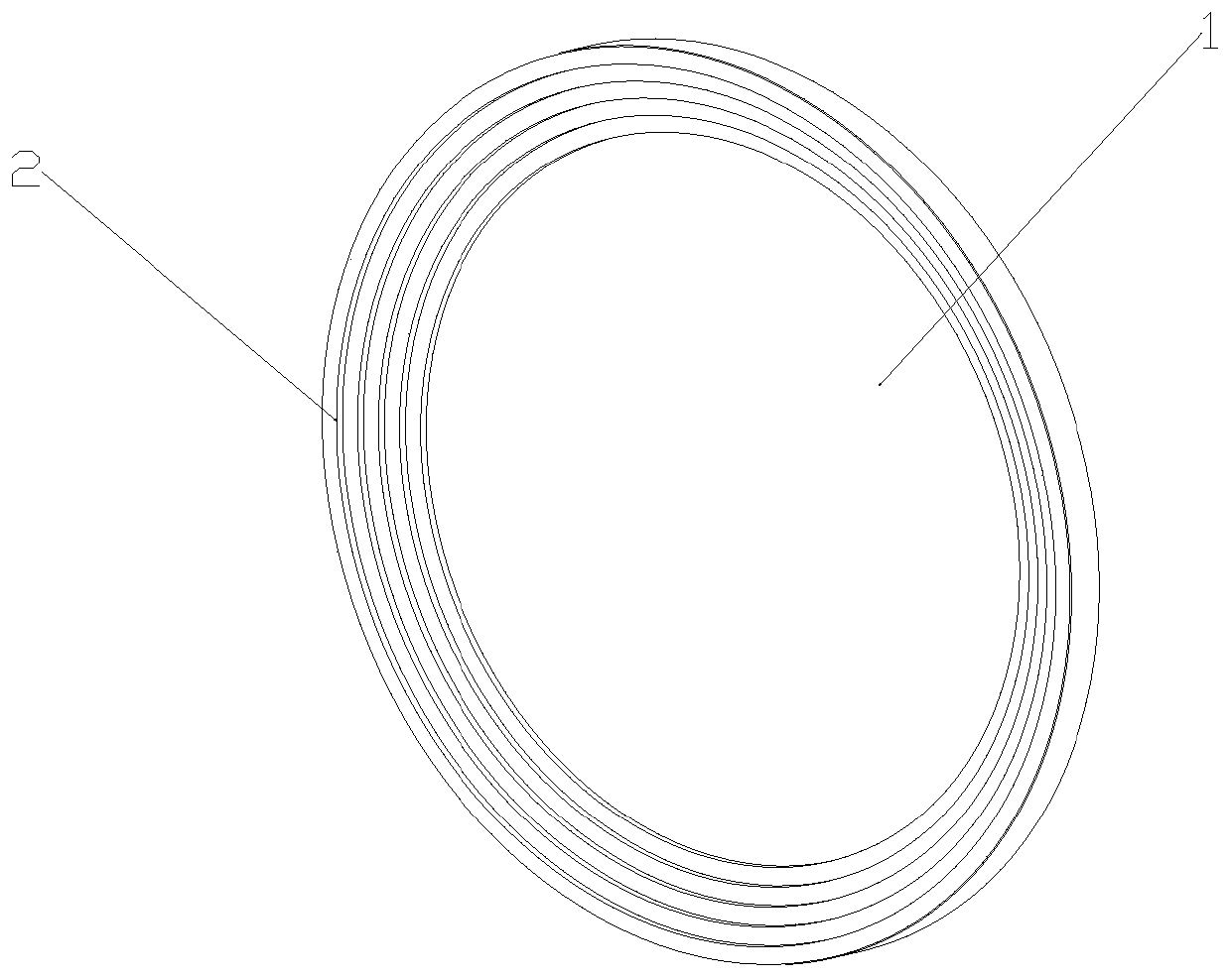
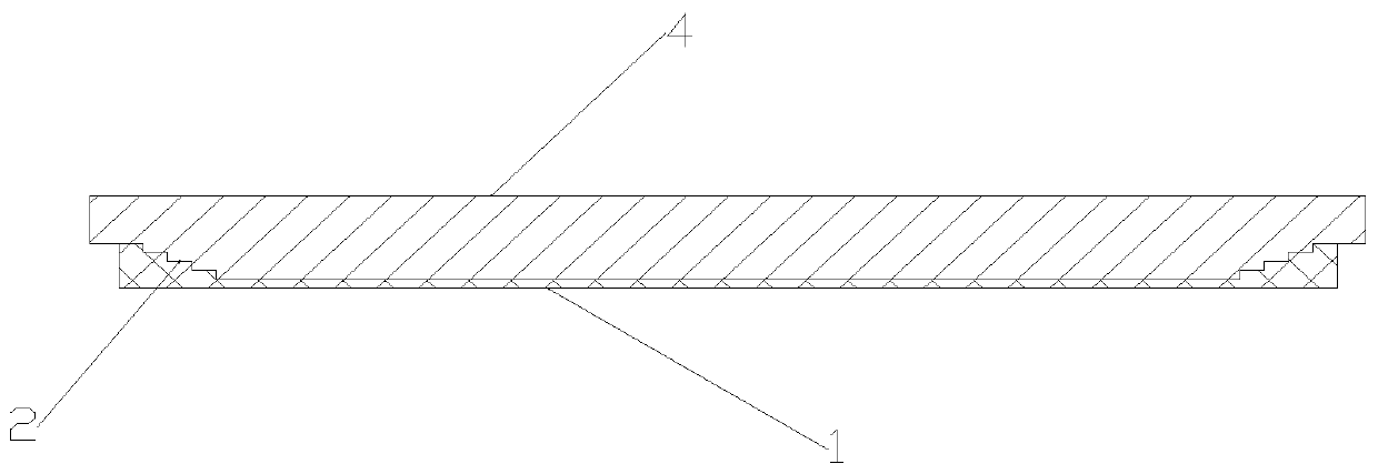

Image

  • Method for completing grain cutting of thin wafer by applying plasma grain cutting and laser equipment
  • Method for completing grain cutting of thin wafer by applying plasma grain cutting and laser equipment
  • Method for completing grain cutting of thin wafer by applying plasma grain cutting and laser equipment

Examples


Embodiment Construction

[0034] The following will clearly and completely describe the technical solutions in the embodiments of the present invention with reference to the accompanying drawings in the embodiments of the present invention. Obviously, the described embodiments are only some, not all, embodiments of the present invention. Based on the embodiments of the present invention, all other embodiments obtained by persons of ordinary skill in the art without creative efforts fall within the protection scope of the present invention.

[0035] In describing the present invention, it is to be understood that the terms "opening", "upper", "lower", "thickness", "top", "middle", "length", "inner", "surrounding" etc. Indicating orientation or positional relationship is only for the convenience of describing the present invention and simplifying the description, and does not indicate or imply that the components or elements referred to must have a specific orientation, be constructed and operated in a sp...


PUM


Abstract

The invention discloses a method for completing grain cutting of a thin wafer by applying plasma grain cutting and laser equipment. The method comprises the steps of adhering the front surface of an ultrathin wafer to a grain cutting frame; coating the upper end of the ultrathin wafer with a water-soluble or organic-soluble transparent polymer; using a laser technology to carry out laser processing on the transparent polymer , and cutting the polymer and the titanium / aluminum copper metal layer through to form a cutting channel pattern; carrying out a plasma process on the ultrathin wafer to cut crystal grains; using DI water / solvent for cleaning and removing polymers and metal impurities left in the laser process; and cutting the crystal grains on a UV type film frame. According to the invention, the coating water-soluble or organic-soluble transparent polymer is used, and a laser and path editing program process is applied, so that a sequence of yellow light processes is reduced; thetransparent polymer is aligned with the cutting channel, so that the cutting process is effectively implemented; and after the metal layer on the cutting channel is cut through by laser to form a polymer cutting channel pattern, the comprehensive plasma process is carried out to cut the crystal grains, and the wafer is not polluted.

Description

technical field [0001] The invention relates to the field of wafer production, in particular to a method for cutting thin wafers by using plasma dicing and laser equipment. Background technique [0002] In the process of wafer processing, it is a current production method to thin the wafer and move and transfer the wafer of 50-100 microns without bonding the carrier plate, and complete the grain cutting process, that is, to grind the wafer Round, generate a wafer with a thickness of 50-200 microns at the bottom of the wafer and leave a frame ring of 3-8 mm on the edge (Taiko Wafer Taiko wafer structure), perform wafer backside thinning and subsequent wafer production processes, and then remove the edge first The ring (Taiko ring) is placed in the cutting film frame, and the grain cutting process is carried out. [0003] Although the existing process method is generally used and can meet the basic thin wafer production requirements, it has the following disadvantages: [00...

Claims


Application Information

Patent Timeline
Patent Type & Authority Applications(China)
IPC IPC(8): H01L21/268H01L21/3065H01L21/302H01L21/78
CPCH01L21/78H01L21/302H01L21/3065H01L21/268
Inventor 严立巍李景贤陈政勋
Owner 绍兴同芯成集成电路有限公司
Why Eureka
Try Eureka