Multi-PLL parallel output clock synchronization system and working method thereof

A technology for outputting clocks and working methods, applied in the direction of electrical components, automatic control of power, etc., can solve the problem of asynchronous multi-PLL parallel output clocks and other problems

Active Publication Date: 2020-07-24
HARBIN INST OF TECH
View PDF8 Cites 2 Cited by
  • Summary
  • Abstract
  • Description
  • Claims
  • Application Information

AI Technical Summary

Problems solved by technology

[0003] The invention provides a multi-PLL parallel output clock synchronization system and its working method, which realizes that after the external synchronization pulse SYNC acts, all output clocks change from inactive level to active level at the same time, and solves the problem of multi-PLL parallel output clock asynchrony The problem

Method used


Image

  • Multi-PLL parallel output clock synchronization system and working method thereof
  • Multi-PLL parallel output clock synchronization system and working method thereof
  • Multi-PLL parallel output clock synchronization system and working method thereof

Examples


Embodiment 1

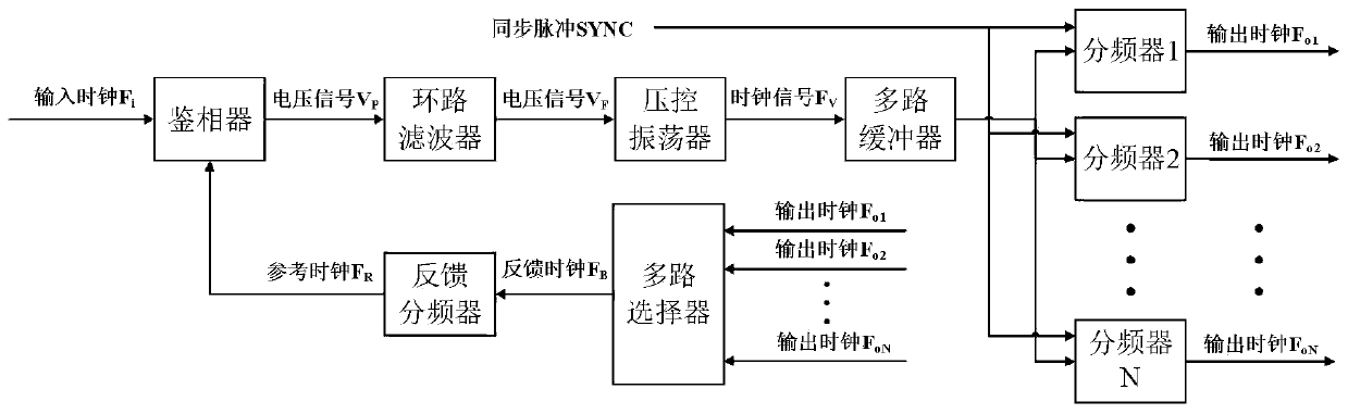
[0030] phase detector on the input clock F i with reference clock F R The frequency of the phase detector is compared with the phase, when both are the same, the voltage signal V output by the phase detector P will be stable; the function of the loop filter is to obtain a voltage signal V with a higher signal-to-noise ratio F ; The core clock F of the voltage-controlled oscillator output PLL work V , its frequency is generally above GHz, and the specific output frequency is determined by the voltage signal V F Control; F V After passing through the multi-channel buffer, and then passing through N frequency dividers respectively, N output clocks are obtained; the multiplexer selects one of the N output clocks as the feedback clock F B , after passing through the feedback frequency divider to get the reference clock F R Send it back to the phase detector, so that the entire PLL forms a complete negative feedback structure.

[0031] The synchronization pulse SYNC is also us...
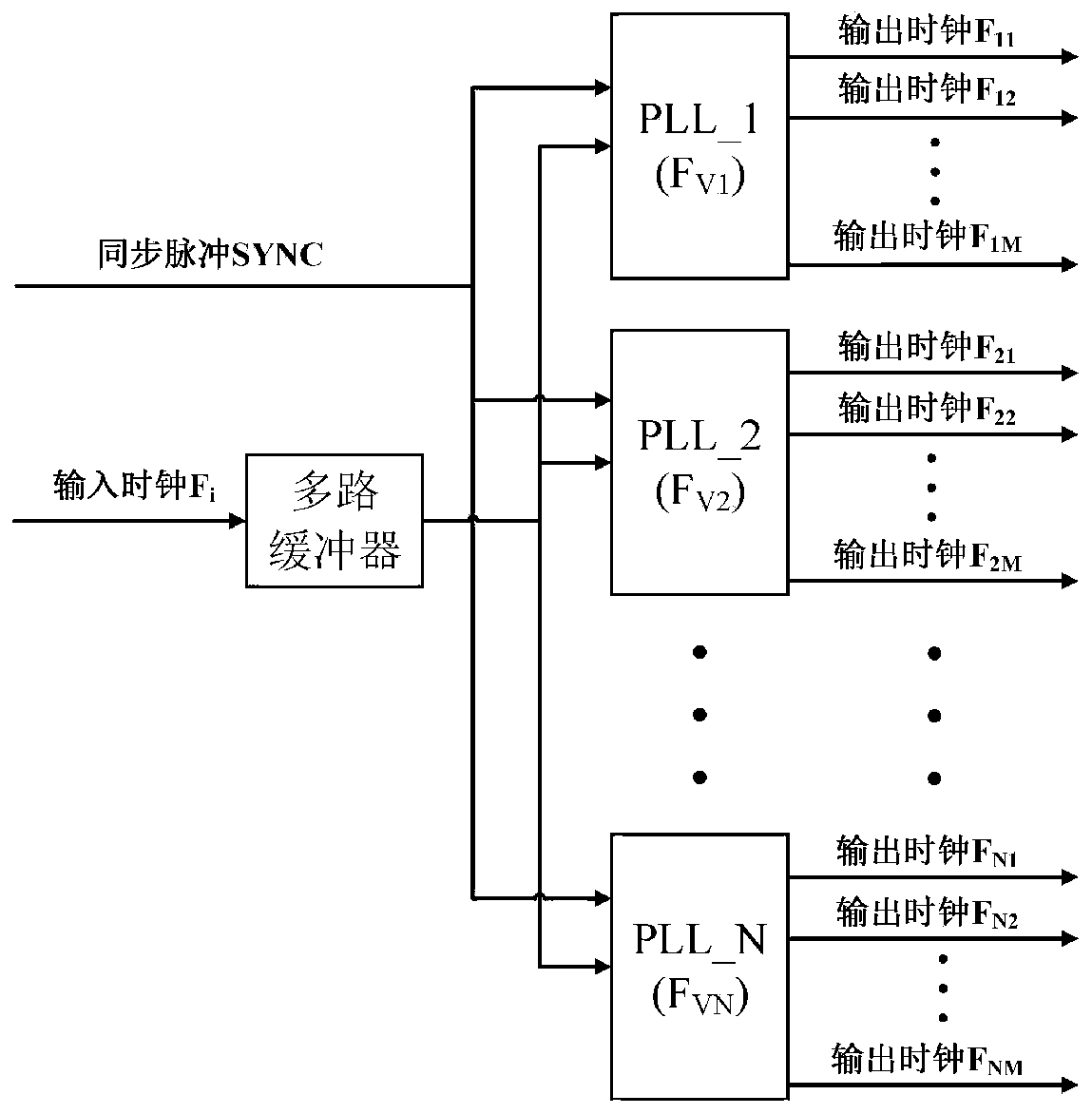
Embodiment 2

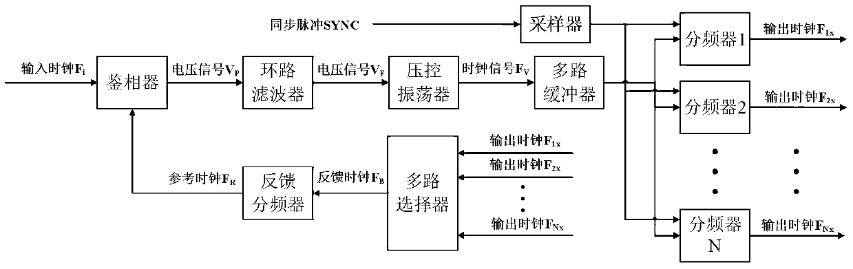
[0053] Such as Figure 4 As shown, for off-the-shelf PLL chips, it provides image 3 in the manner required by the sampler circuit. Figure 4 The specific implementation structure of the digital circuit is given, which is composed of a clock multiplexer and a sampling flip-flop. This structure is added to the ready-made PLL chip, and it can be re-made.

Embodiment 3

[0055] For programmable logic devices such as FPGA, while synchronous PLL is integrated inside, it can be programmed on-site by using hardware description language to realize image 3 The sampler circuit shown.


PUM


Abstract

The invention provides a multi-PLL parallel output clock synchronization system and a working method thereof. The method comprises the following steps: step 1, after a circuit completes phase lockingand reaches a stable state, the working frequencies of all VCO clock signals FV1 to FVN are the same; 2, configuring frequency dividers in all PPLs to enable the frequency of an output clock of a first channel of each PLL to be the same as the frequency of an input clock Fi, and selecting the output clock of the first channel for each PLL from a multiplexer to serve as a feedback clock for phase locking; step 3, when all PLLs complete phase locking and reach a stable state, configuring an output frequency divider 1 in each PLL to be not affected by SYNC; step 4, adding a sampler circuit on aninput path of SYNC; and step 5, the SYNC sends out effective pulses, and edge synchronization is realized after PLL synchronization. According to the invention, all output clocks are changed from invalid levels to valid levels at the same moment after the action of the external SYNC.

Description

technical field [0001] The invention belongs to the technical field of digital circuits; in particular, it relates to a multi-PLL parallel output clock synchronization system and a working method thereof. Background technique [0002] Clock phase-locked loop (Phase Locked Loop, PLL) plays an important role in modern electronic systems. In digital integrated circuits, PLLs are often used to synthesize clock signals of different frequencies required by the chip. The PLL usually consists of a phase detector (Phase Detector, PD), a loop filter (Loop Filter, LF), and a voltage-controlled oscillator (Voltage Controlled Oscillator, VCO). path. N different frequency dividers can be connected behind the voltage-controlled oscillator to realize N clock outputs with different frequencies, and solve the problem of asynchronous output clocks of multiple PLLs connected in parallel. Contents of the invention [0003] The invention provides a multi-PLL parallel output clock synchroniza...

Claims


Application Information

Patent Timeline
Patent Type & Authority Applications(China)
IPC IPC(8): H03L7/07H03L7/08H03L7/091
CPCH03L7/07H03L7/0805H03L7/091Y02D10/00
Inventor 乔家庆王振宇刘冰王华辰陈帅
Owner HARBIN INST OF TECH
Why Eureka
Try Eureka