Wafer repasting device

A technology for wafer transfer and equipment, which is used in the manufacture of conveyor objects, electrical components, semiconductor/solid-state devices, etc., and can solve problems such as chipping, product loss, and high movement risk

Pending Publication Date: 2020-08-04
NANTONG TONGFU MICROELECTRONICS CO LTD
View PDF3 Cites 2 Cited by
  • Summary
  • Abstract
  • Description
  • Claims
  • Application Information

AI Technical Summary

Problems solved by technology

[0002] The gallium arsenide wafer operation needs to transfer the gallium arsenide wafer to the designated blue film for the wafer loading process. At present, the incoming materials of the gallium arsenide wafer are fixed and protected by the mother ring, and the product has been ground, cut and pasted on the On the dicing film, you only need to transfer the product on the designated blue film for the film loading process. Since there is no such transfer equipment in the industry, the current mass-produced products are manually transferred, and the risk of action is high and often occurs. Accidents such as wafer dropping, chip scratching, loss, and collapse directly cause product loss

Method used


Image

  • Wafer repasting device
  • Wafer repasting device
  • Wafer repasting device

Examples


Embodiment Construction

[0032] The application will be further described in detail below in conjunction with the accompanying drawings and embodiments. It should be understood that the specific embodiments described here are only used to explain related inventions, rather than to limit the invention. It should also be noted that, for ease of description, only parts related to the invention are shown in the drawings.

[0033] It should be noted that, in the case of no conflict, the embodiments in the present application and the features in the embodiments can be combined with each other. The present application will be described in detail below with reference to the accompanying drawings and embodiments.

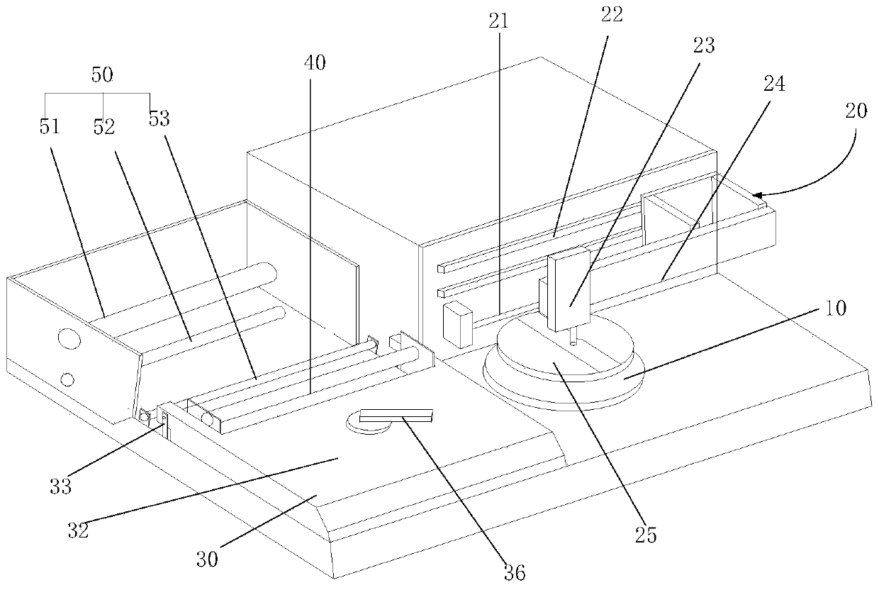
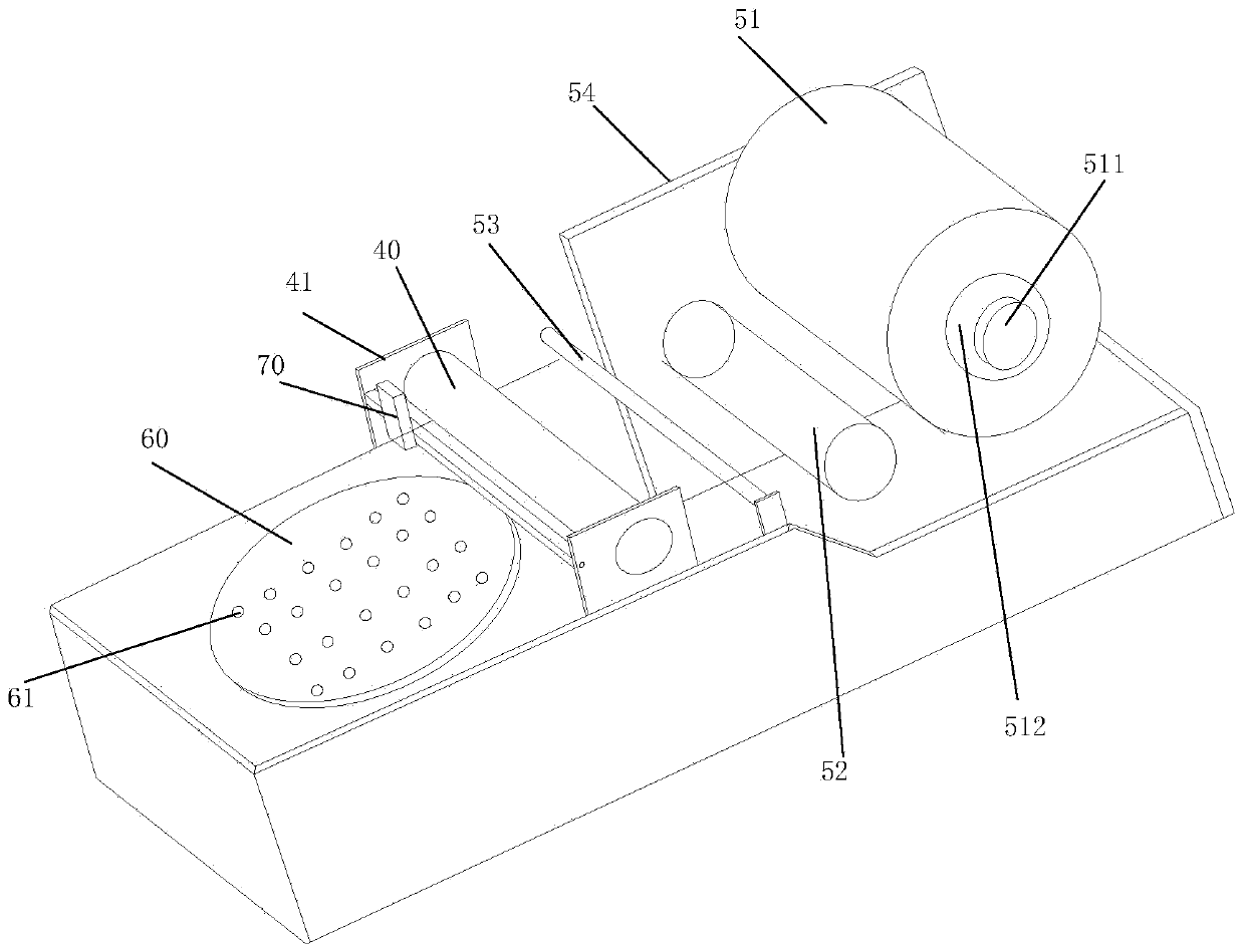
[0034] Such as figure 1 , figure 2 As shown, the present application discloses a wafer transfer device, comprising: a first transfer table 60 for placing a wafer to be pasted with a blue film; a roller 40 slidably arranged on the first transfer table 60 Above, it is used to roll the blue film t...


PUM


Abstract

The invention discloses a wafer repasting device. The wafer repasting device comprises a first repasting table disc, a roller arranged over the first repasting table disc in a sliding mode, a blue film cutting assembly arranged over the first repasting table disc, and a carrying unit used for carrying a wafer on the first repasting table disc to a second repasting table disc and pressing the waferdownwards to enable a blue film to be firmly pasted to the wafer. The blue film cutting assembly can be switched between the position close to the first repasting table disc and the position far awayfrom the first repasting table disc and is used for cutting the blue film along the outline of a primary-secondary ring. The wafer repasting device provided by the invention is simple in structure, convenient to operate, stable in equipment operation, simple to maintain and low in cost; during work, repasting of the wafer can be completed only through manual feeding and discharging, pure manual operation is replaced, the risk of manual operation is reduced to a great extent, and therefore the repasting quality of the wafer is guaranteed, and the production efficiency is greatly improved.

Description

technical field [0001] The invention generally relates to the technical field of semiconductors, and in particular to a wafer transfer device. Background technique [0002] The gallium arsenide wafer operation needs to transfer the gallium arsenide wafer to the designated blue film for the wafer loading process. At present, the incoming materials of the gallium arsenide wafer are fixed and protected by the mother ring, and the product has been ground, cut and pasted on the On the dicing film, you only need to transfer the product on the designated blue film for the film loading process. Since there is no such transfer equipment in the industry, the current mass-produced products are manually transferred, and the risk of action is high and often occurs. Accidents such as wafer dropping, chip scratching, loss, and collapse directly cause product loss. Contents of the invention [0003] In view of the above defects or deficiencies in the prior art, it is desired to provide a...

Claims


Application Information

Patent Timeline
Patent Type & Authority Applications(China)
IPC IPC(8): H01L21/67H01L21/677
CPCH01L21/67132H01L21/67703
Inventor 薛超
Owner NANTONG TONGFU MICROELECTRONICS CO LTD
Why Eureka
Try Eureka