High-erasing-speed semi-floating-gate memory and preparation method thereof

A technology of erasing and writing speed and semi-floating gate, which is applied in semiconductor/solid-state device manufacturing, semiconductor devices, electric solid-state devices, etc. The effect of small contact resistance and increased gate capacitance

Active Publication Date: 2020-08-04
FUDAN UNIV +1
View PDF9 Cites 2 Cited by
  • Summary
  • Abstract
  • Description
  • Claims
  • Application Information

AI Technical Summary

Problems solved by technology

In addition, as the size of the transistor continues to shrink, the opening where the source of the tunneling transistor is also shrinking, which causes the contact resistance at the opening to increase, thereby reducing the speed of the tunneling transistor

Method used


Image

  • High-erasing-speed semi-floating-gate memory and preparation method thereof
  • High-erasing-speed semi-floating-gate memory and preparation method thereof
  • High-erasing-speed semi-floating-gate memory and preparation method thereof

Examples


Embodiment Construction

[0039] The present invention will be further introduced below in conjunction with the embodiments and accompanying drawings. It should be understood that the examples are only used to explain the present invention, not to limit the present invention. All other embodiments obtained by persons of ordinary skill in the art without creative efforts fall within the protection scope of the present invention.

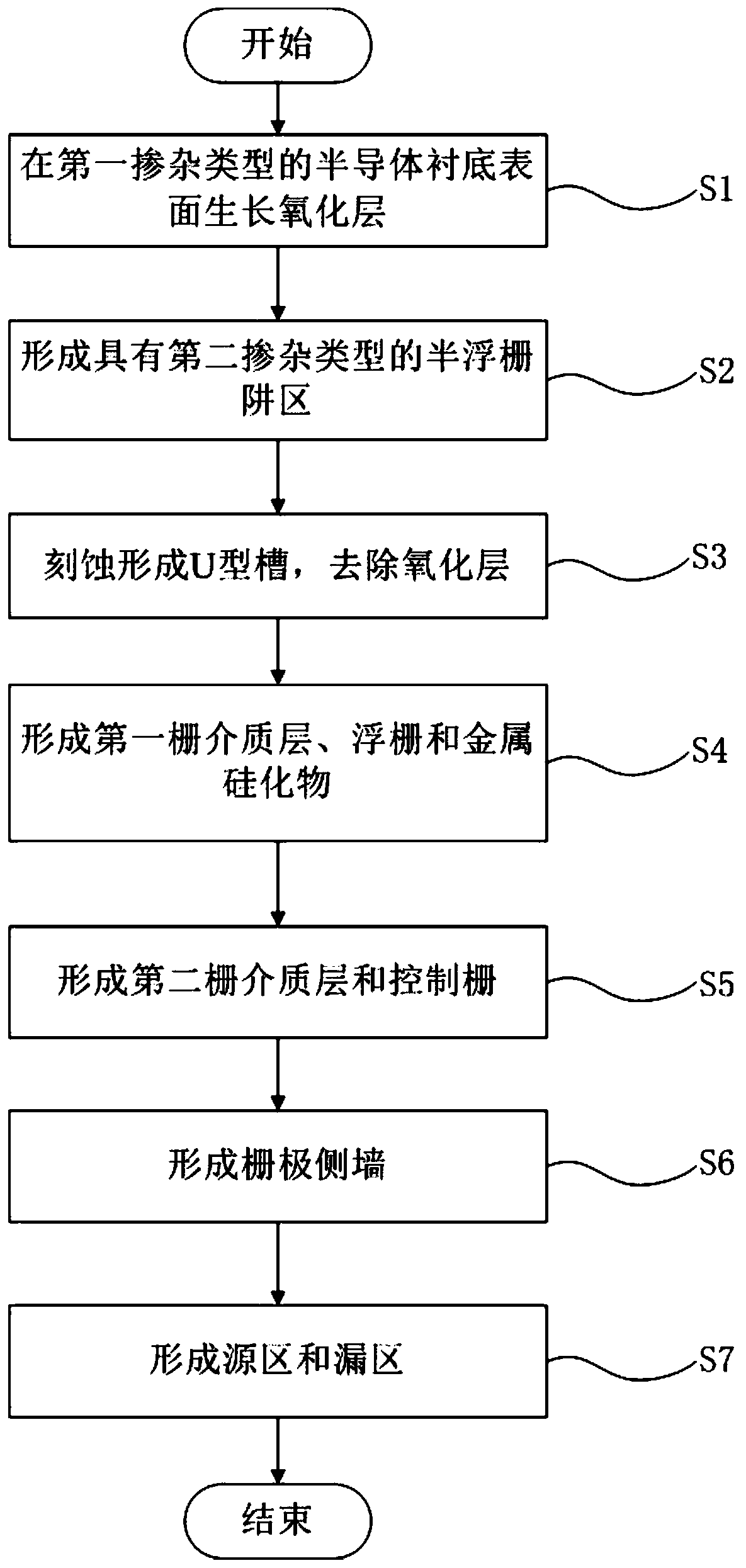
[0040] figure 1 It is a flow chart of the preparation method of the high erasing and writing speed semi-floating gate memory. Figure 2-15 A structural schematic diagram showing each step of the method for manufacturing the high erasing and writing speed semi-floating gate memory. Such as figure 1 As shown, the specific preparation steps are:

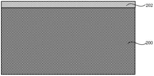
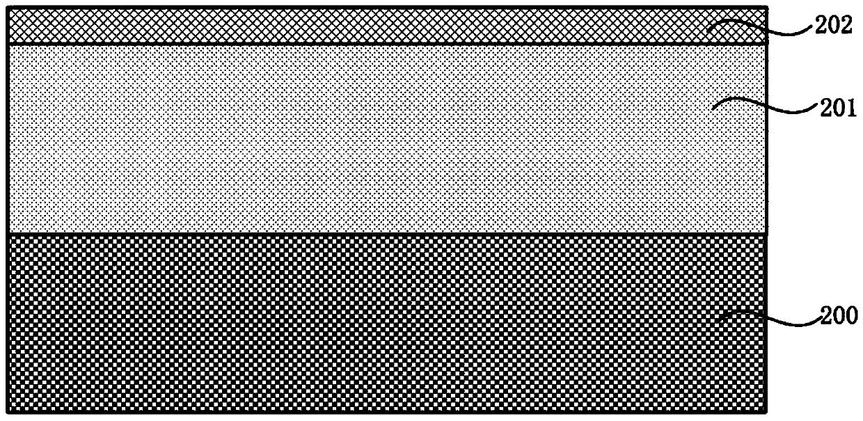
[0041] Step S1, providing a silicon-containing semiconductor substrate 200 with a first doping type. The silicon-containing semiconductor substrate 200 is, for example, a bulk semiconductor substrate such as Si, SiGe, a semiconduct...


PUM


Abstract

The invention belongs to the technical field of integrated circuit memories, and particularly relates to a high-erasing-speed semi-floating-gate memory and a preparation method thereof. The semi-floating-gate memory comprises a silicon-containing semiconductor substrate having a first doping type, a semi-floating-gate well region which has a second doping type, and a U-shaped groove which penetrates through the semi-floating-gate well region, wherein the bottom of the U-shaped groove is located at the lower boundary of the semi-floating-gate well region; a first gate dielectric covers the surface of the U-shaped groove, and an opening is formed in the semi-floating-gate well region; a floating gate covers the first gate dielectric, and a metal silicide is formed in the semi-floating-gate well region below the opening; a second gate dielectric layer wraps the floating gate, and a control gate covers the second gate dielectric layer; gate side walls are positioned on the two sides of a first gate stack and a second gate stack; and a source region and a drain region have a second doping type and are positioned on two sides of the first gate stack and the second gate stack. According to the invention, the erasing speed of the memory can be increased, the contact resistance of the source electrode of a tunneling transistor is obviously reduced, the driving current of the tunneling transistor is increased, and the erasing speed of the memory is further increased.

Description

technical field [0001] The invention belongs to the technical field of integrated circuit memory, and in particular relates to a high erasing and writing speed semi-floating gate memory and a preparation method thereof. Background technique [0002] At present, the DRAM devices used in integrated circuit chips are mainly 1T1C structures, that is, a transistor is connected in series with a capacitor, and the capacitor is charged and discharged through the switching of the transistor, thereby realizing the conversion between 0 and 1 of the DRAM device. As the device size becomes smaller and smaller, DRAM devices used in integrated circuit chips are facing more and more problems. For example, DRAM devices require 64ms refresh time, so the capacitance value of the capacitor must be kept above a certain value to ensure a long enough time. However, with the shrinking of the feature size of integrated circuits, the manufacture of large capacitors has become more and more difficult,...

Claims


Application Information

Patent Timeline
Patent Type & Authority Applications(China)
IPC IPC(8): H01L27/108H01L29/49H01L29/51H01L21/8242
CPCH01L29/517H01L29/495H10B12/20H10B12/01
Inventor 朱宝陈琳孙清清张卫
Owner FUDAN UNIV
Why Eureka
Try Eureka