Supercharge Your Innovation With Domain-Expert AI Agents!

Power module

A technology of power modules and power devices, which is applied to printed circuits connected with non-printed electrical components, non-metallic protective layer coating, and printed circuit manufacturing. It can solve the problem of power control and conversion that cannot achieve high frequency and high efficiency. problem, to avoid high cost, reduce the connection distance, and avoid the effect of single function

Pending Publication Date: 2020-08-07
苏州量芯微半导体有限公司
View PDF0 Cites 0 Cited by
  • Summary
  • Abstract
  • Description
  • Claims
  • Application Information

AI Technical Summary

Problems solved by technology

Traditional silicon power modules are usually IGBTs plus fast recovery diodes. Due to the limitations of materials and device structures, it is impossible to achieve high-frequency and high-efficiency power control and conversion.

Method used


Image

  • Power module
  • Power module
  • Power module

Examples


Embodiment Construction

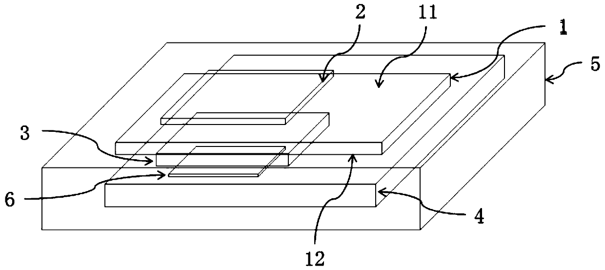
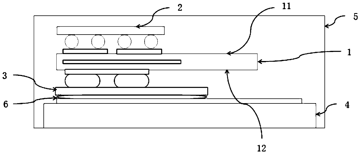
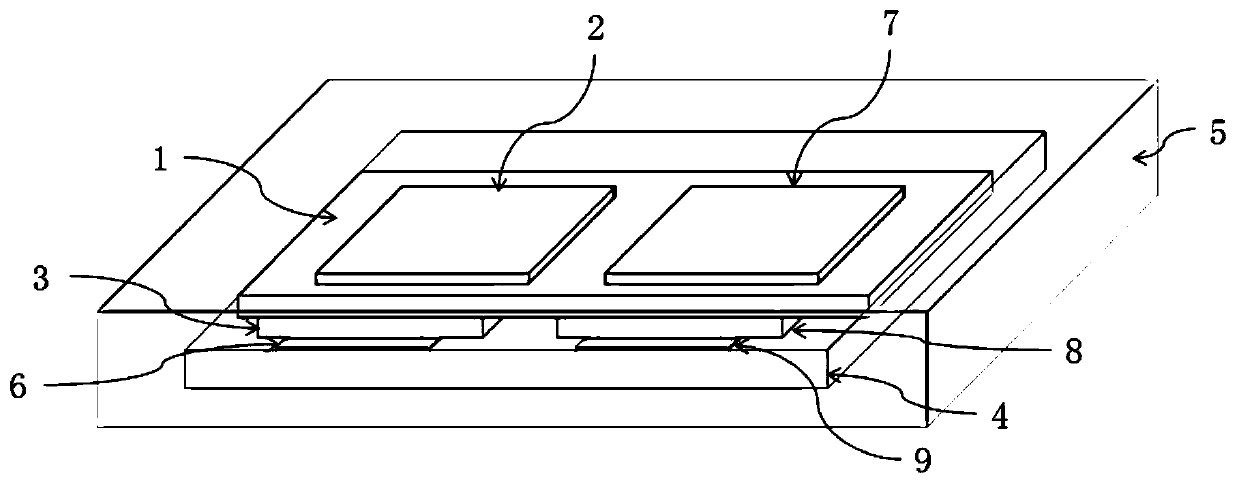
[0034] The details of the present invention can be understood more clearly with reference to the accompanying drawings and the description of specific embodiments of the present invention. However, the specific embodiments of the present invention described here are only for the purpose of explaining the present invention, and should not be construed as limiting the present invention in any way. Under the teaching of the present invention, the skilled person can conceive any possible modification based on the present invention, and these should be regarded as belonging to the scope of the present invention. It should be noted that when an element is referred to as being “disposed on” another element, it may be directly on the other element or there may also be an intervening element. When an element is referred to as being "connected to" another element, it can be directly connected to the other element or intervening elements may also be present. The terms "mounted", "connec...


PUM


Abstract

The invention, which relates to the technical field of the semiconductor, discloses a power module comprising a printed circuit board having a first surface for installing an electronic component device and a second surface corresponding to the first surface; a first driving chip mounted on the first surface of the printed circuit board; a first gallium nitride power device arranged on the secondsurface of the printed circuit board; a copper-clad ceramic substrate arranged on one surface, deviating from the printed circuit board, of the first gallium nitride power device; and a packaging plastic used for packaging the printed circuit board, the first driving chip, the first gallium nitride power device and the copper-clad ceramic substrate, and exposed out of one surface, deviating from the first gallium nitride power device, of the copper-clad ceramic substrate. The position of the first gallium nitride power device is opposite to the position of the first driving chip. Parasitic parameters can be effectively reduced, the electric energy conversion efficiency is improved, and the power density of the whole module is improved.

Description

technical field [0001] The invention relates to the technical field of semiconductors, in particular to a power module. Background technique [0002] Gallium nitride is known as the representative material of the third generation semiconductor. In power devices, compared with silicon devices, gallium nitride devices can perform high-frequency (up to 500KHz~1MHz) and extremely low-loss switching at high voltages, reduce the cost of the entire power system, improve conversion efficiency, and have more High power density, smaller size and better heat dissipation. In the field of small and medium power adapters, GaN-based adapters have achieved mass production and are expected to fully replace silicon in some areas in the near future. Discrete gallium nitride drivers will bring new challenges to PCB layout, because the switching speed of gallium nitride is very fast, and the parasitic parameters of the additional drive circuit will inevitably cause voltage and current oscillat...

Claims


Application Information

Patent Timeline
IPC IPC(8): H01L25/16H01L23/498H05K1/18H05K3/28
CPCH01L23/49838H01L25/16H05K1/181H05K3/284H01L2224/16225H01L2924/181H01L2924/00012
Inventor 傅玥李湛明高卫东吴伟东
Owner 苏州量芯微半导体有限公司
Features
  • R&D
  • Intellectual Property
  • Life Sciences
  • Materials
  • Tech Scout
  • Unparalleled Data Quality
  • Higher Quality Content
  • 60% Fewer Hallucinations
Learn More