
Raised Pad manufacturing method

A production method and operation technology, applied in the field of press bearings, can solve the problems of increasing production costs, using a large amount of ink, and low production efficiency, and achieving the effect of shortening production time, reducing the use of ink, and improving product yield.

Active Publication Date: 2020-08-07
VICTORY GIANT TECH HUIZHOU CO LTD
View PDF5 Cites 6 Cited by
  • Summary
  • Abstract
  • Description
  • Claims
  • Application Information

AI Technical Summary

Problems solved by technology

This kind uses dry film to seal the hole, plus screen printing wet film to make the outer layer circuit process. The production yield is about 60% to 70%, and the entire outer layer circuit process requires 18 processes, and screen printing is generally time-consuming. It takes about 3 hours, the process is complicated and time-consuming, the overall production efficiency is low, and a large amount of ink needs to be used during screen printing, which consumes more materials and increases the production cost

Method used


Image

  • Raised Pad manufacturing method

Examples


Embodiment Construction

[0033] The method for making the Raised Pad of the present invention will be further described in detail below in conjunction with specific embodiments and accompanying drawings.

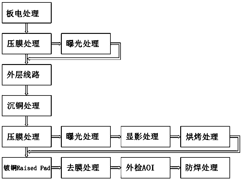
[0034] refer to figure 1 According to a non-limiting embodiment of the present invention, a method for manufacturing a Raised Pad includes manufacturing an outer layer circuit, and the manufacturing of the outer layer circuit includes the following steps.

[0035] S1: Board electroplating treatment. After the PCB board is drilled for the inner layer, it enters the board electroplating process, and the entire board is electroplated by electroplating, so that the entire board surface and the walls of the drilled holes are coated with a layer of metal copper, increasing the board surface and The thickness of the copper layer on the hole wall is used to connect the inner layers of the circuit and realize multi-layer interconnection. The plate electrical treatment is produced by copper plating through a ...


PUM

PropertyMeasurementUnit
thicknessaaaaaaaaaa

Abstract

The invention relates to a Raised Pad manufacturing method, which comprises the steps of manufacturing an outer layer circuit, and the manufacturing of the outer layer circuit comprises the followingsteps of: S1, drilling the inner layer circuit of a PCB, entering a board electrical process, electroplating the whole board in an electroplating mode, and plating a layer of copper on the whole boardsurface and the wall of a drilled hole; S2, pressing a layer of photosensitive anti-corrosion film on the board surface subjected to plate electrification by using a hot roller film pressing machineto ensure the copper plating thickness; S3, manufacturing an outer layer circuit by adopting a developing machine, an etching machine and a film removing machine; S4, depositing a thin copper layer onthe independent units of the outer-layer circuit through copper deposition wires to enable the independent units to be connected together, and providing a conductor for subsequent electroplating; S5,pressing a layer of photosensitive anti-corrosion film on the board surface subjected to plate electrification by using a hot roller film pressing machine for manufacturing a PAD pattern for electroplating; and S6, placing the treated board on a copper plating wire to be subjected to copper plating operation, and obtaining the Raided Pad. The Raised Pad manufacturing method has the advantages ofthe simple process, low cost, high efficiency, the good product yield and the like.

Description

technical field [0001] The invention relates to the technical field of pressure bearings, in particular to a method for making a Raised Pad. Background technique [0002] Rasied PAD (raised pad) technology is one of the main application technologies of the next-generation PCB server CPU control module substrate. This type of product meets the market product development needs of AMD and other major customers, and its application prospect is broad. The wide range of product applications comes from its technological innovation and stable performance. The technical index of Raised PAD is higher than that of conventional PCB. The BGA area of ​​conventional PCB is exposed to the pad PAD through the solder mask window, so the PAD is lower than the solder mask layer. The Rasied PAD board is plated with copper to set a PAD height of 2mil, and the height of the finished product is 25um higher than the thickness of the green oil. Its purpose is to provide a good soldering platform fo...

Claims


Application Information

Patent Timeline
Patent Type & Authority Applications(China)
IPC IPC(8): H05K3/00H05K3/10H05K3/18H05K3/22C25D7/00C25D3/38
CPCC25D3/38C25D7/00H05K3/00H05K3/0011H05K3/0085H05K3/10H05K3/18H05K3/22
Inventor 吴柳松夏国伟张军杰吕海李剑华
Owner VICTORY GIANT TECH HUIZHOU CO LTD
Learn More