Technological method for improving recoverability of silicon wafer through adoption of high-temperature wet oxygen oxidation method
A technology of wet oxygen oxidation and process method, which is applied in the direction of electrical components, semiconductor/solid-state device manufacturing, circuits, etc., can solve the problems of low recycling efficiency and difficult removal, achieve high-efficiency recycling, increase the number of recycling and reuse, and improve The effect of recyclability
- Summary
- Abstract
- Description
- Claims
- Application Information
AI Technical Summary
Problems solved by technology
Method used
Image

Examples
Embodiment 1
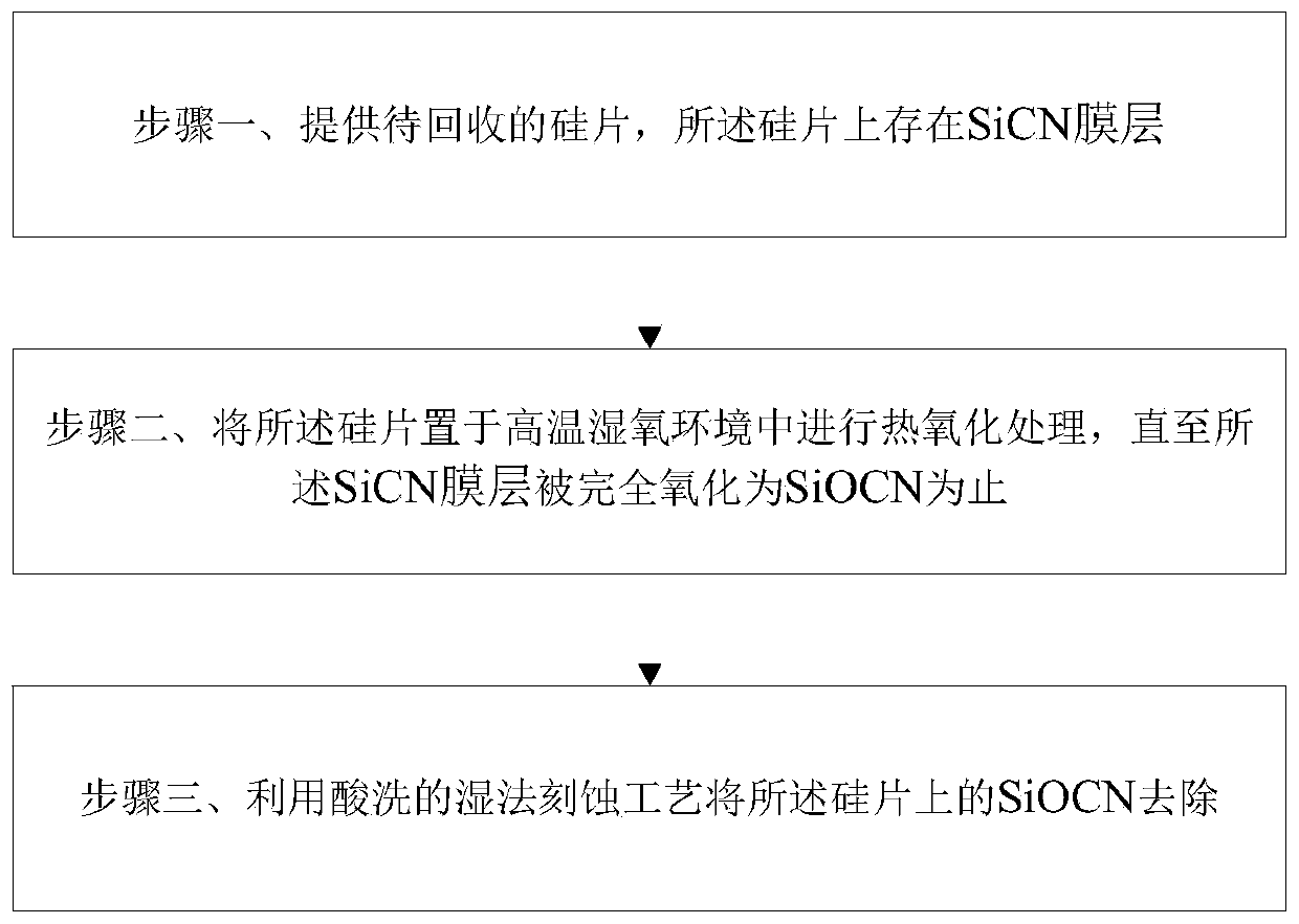
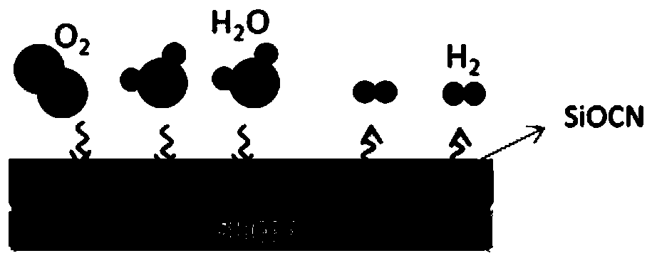
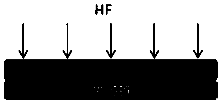
[0027] The invention provides a process for improving the recyclability of silicon wafers through high temperature wet oxygen oxidation, such as figure 1 as shown, figure 1 It is shown as a schematic flow chart of the process method for improving the recyclability of silicon wafers through the high temperature wet oxygen oxidation method of the present invention. The steps of the process method in this embodiment are as follows:
[0028] Step 1: providing a silicon wafer to be recovered, on which there is a SiCN film layer; further in the present invention, the SiCN film layer in step 1 exists on both sides of the silicon wafer to be recovered. Since the SiCN film layer on the silicon wafer usually has an anti-corrosion effect in the integrated circuit manufacturing process, the formed SiCN film layer is generally used as the side wall of the gate. When the silicon wafer is recycled, the front and back sides of the silicon wafer The SiCN film layer needs to be removed to hav...
Embodiment 2
[0032] This embodiment provides a method for improving the recyclability of silicon wafers by high-temperature wet oxygen oxidation, such as figure 1 As shown, Figure 1 shows a schematic flow chart of the process method for improving the recyclability of silicon wafers through high-temperature wet oxygen oxidation according to the present invention. The steps of the process method in this embodiment are as follows:
[0033] Step 1: providing a silicon wafer to be recovered, on which there is a SiCN film layer; further in the present invention, the SiCN film layer in step 1 exists on both sides of the silicon wafer to be recovered. Since the SiCN film layer on the silicon wafer usually has an anti-corrosion effect in the integrated circuit manufacturing process, the formed SiCN film layer is generally used as the side wall of the gate. When the silicon wafer is recycled, the front and back sides of the silicon wafer The SiCN film layer needs to be removed to have recycling valu...
PUM
 Abstract
Description
Claims
Application Information