

Display substrate, manufacturing method thereof and display device
A display substrate and manufacturing method technology, applied in semiconductor devices, electrical components, circuits, etc., can solve problems such as general climbing ability, breakage, poor display, etc., and achieve the effect of ensuring connection reliability and product yield
- Summary
- Abstract
- Description
- Claims
- Application Information
AI Technical Summary
Problems solved by technology
Method used
Image

Examples
Embodiment Construction
[0034] In order to make the technical problems, technical solutions and advantages to be solved by the embodiments of the present invention clearer, the following will describe in detail with reference to the drawings and specific embodiments.
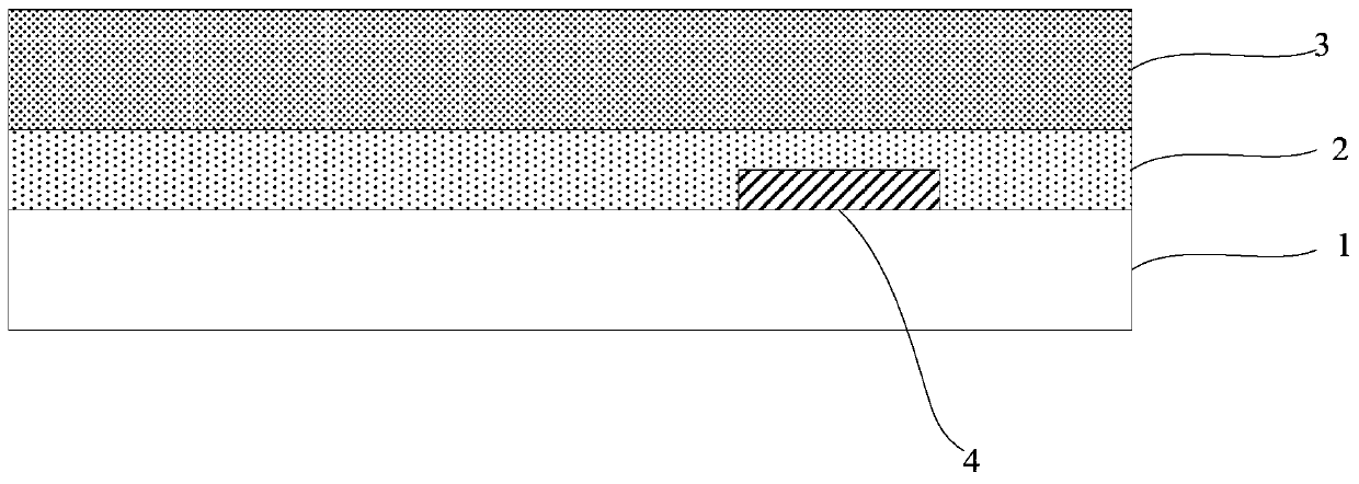
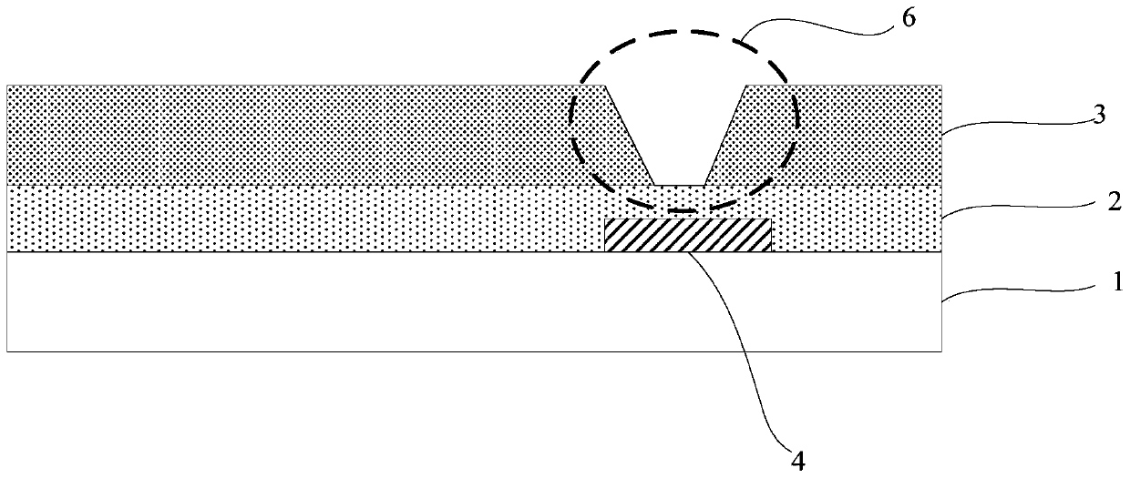
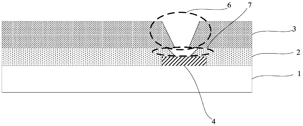
[0035] In the manufacturing process of OLED display devices, after the passivation layer is deposited, a flat layer needs to be deposited. The flat layer can be made of photosensitive acrylic material, and the flat layer is exposed and developed to form the first via hole through the flat layer; Form a photoresist on the photoresist, expose and develop the photoresist to form a pattern of the photoresist, use the pattern of the photoresist as a mask, etch the passivation layer, and form the first passivation layer through the dry etching process Two vias. The depth of the second via hole is relatively large, and the slope angle of the second via hole formed after the dry etching process is generally 80-90°. When ITO is subsequently dep...
PUM
 Abstract
Description
Claims
Application Information