
Adjustable surface enhanced Raman scattering substrate

A surface-enhanced Raman and substrate technology, applied in the direction of Raman scattering, measuring devices, instruments, etc., can solve the problems of inconvenient use, output wavelength mismatch, and non-adjustable shape, and achieve good application prospects, enhanced strength, Adjust the effect of high sensitivity

Inactive Publication Date: 2020-08-18
西安柯莱特信息科技有限公司
View PDF0 Cites 2 Cited by
  • Summary
  • Abstract
  • Description
  • Claims
  • Application Information

AI Technical Summary

Problems solved by technology

After the noble metal micro-nano structure is prepared, the shape cannot be adjusted. Often due to experimental errors, the inherent vibration wavelength of the prepared noble metal micro-nano structure does not match the output wavelength of the existing laser, so it often causes inconvenience to use.

Method used


Image

  • Adjustable surface enhanced Raman scattering substrate
  • Adjustable surface enhanced Raman scattering substrate
  • Adjustable surface enhanced Raman scattering substrate

Examples


Embodiment 1

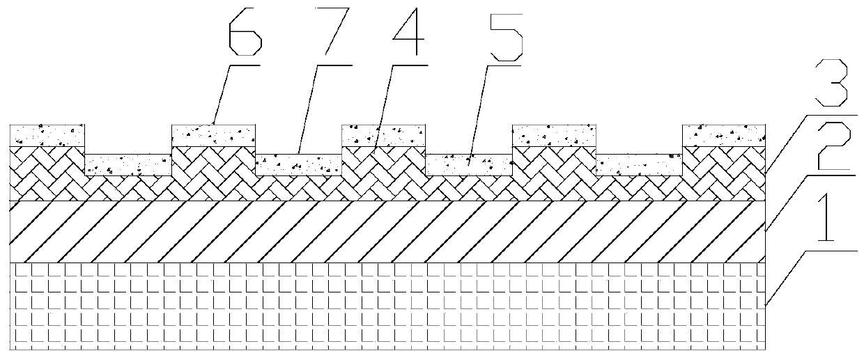
[0020] The present invention provides a tunable surface-enhanced Raman scattering substrate, such as figure 1 As shown, the surface-enhanced Raman scattering substrate includes a substrate 1, an elastic layer 2, a magnetostrictive layer 3, a magnetostrictive material protrusion 4, a magnetostrictive material depression 5, a noble metal protrusion 6, and a noble metal depression 7 . The elastic layer 2 is placed on the substrate 1, and the substrate 1 can be silicon dioxide or silicon. The magnetostrictive layer 3 is placed on the elastic layer 2, and the upper surface of the magnetostrictive layer 3 is provided with periodically arranged magnetostrictive material protrusions 4 and magnetostrictive material depressions 5, and the noble metal protrusions 6 are arranged on the magnetostrictive layer. On the material protrusion 4 , a noble metal recess 7 is arranged on the magnetostrictive material recess 5 . The material of the noble metal protrusions 6 and the noble metal depr...

Embodiment 2

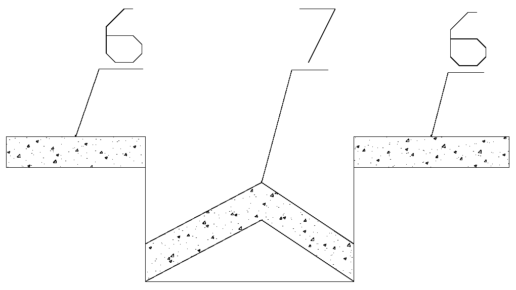
[0026] On the basis of Example 1, such as figure 2 As shown, the magnetostrictive material concave portion 5 is circular, and the bottom surface of the magnetostrictive material concave portion 5 is provided with a protruding portion. The noble metal depression 7 also has a protrusion, that is, the center of the noble metal depression 7 is high and the edge is low. This is beneficial to enhance the coupling between the central position of the noble metal recessed part 7 and the noble metal protruding part 6 under the excitation of the incident light, forming stronger resonance and generating a stronger electric field. On the other hand, the lower edges of the noble metal recesses 7 are beneficial to store more molecules to be detected at these positions, and are beneficial to increase the intensity of surface-enhanced Raman scattering signals.

Embodiment 3

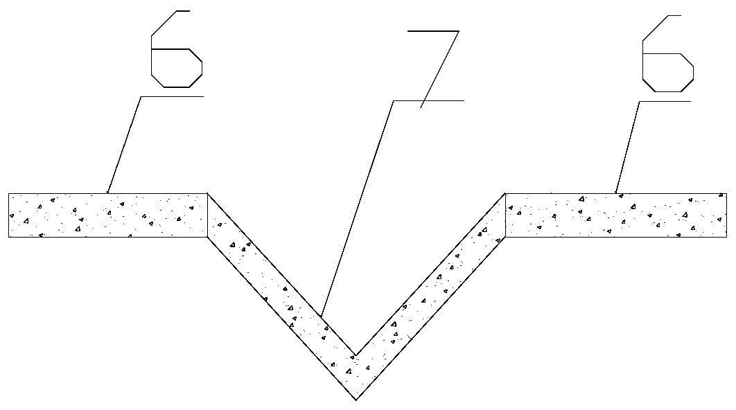
[0028] On the basis of Example 1, such as image 3 As shown, the protrusions 4 of the magnetostrictive material and the recesses 5 of the magnetostrictive material are strip-shaped, that is, the structure has a strip-shaped period. The magnetostrictive material recess 5 is wedge-shaped, and the thickness of the noble metal recess 5 is the same at different positions. Such as image 3 As shown, a wedge-shaped groove is formed in the noble metal recess 7, the groove is beneficial to gather the molecules to be measured, and a strong electric field is formed in the groove to increase the intensity of the surface-enhanced Raman scattering signal.


PUM


Abstract

The invention provides an adjustable surface enhanced Raman scattering substrate, a magnetostriction material is arranged on an elastic layer, and a precious metal micro-nano structure is arranged onthe magnetostriction material. Under the action of a magnetic field, the magnetostrictive material expands or contracts. Therefore, the morphology of the precious metal micro-nano structure or the distance between the precious metal micro-nano structures is changed; according to the surface enhanced Raman scattering device, the noble metal micro-nano structure is adopted to change the natural vibration frequency of the noble metal micro-nano structure, so that the natural vibration frequency is matched with the vibration frequency of incident light, a stronger local electric field is generatednear the noble metal micro-nano structure, and finally, the strength of surface enhanced Raman scattering signals is enhanced. Due to the fact that the vibration frequency of the precious metal micro-nano structure is very sensitive to the morphology or spacing of the precious metal micro-nano structure, the vibration frequency of the precious metal micro-nano structure can be well regulated andcontrolled by applying the magnetostrictive material, and the magnetostrictive material has the advantage of being high in adjustment sensitivity and has a good application prospect in the aspect of surface enhanced Raman scattering substrate preparation.

Description

technical field [0001] The invention relates to the field of surface-enhanced Raman scattering, in particular to an adjustable surface-enhanced Raman scattering substrate. Background technique [0002] Surface-enhanced Raman scattering uses the local electric field on the surface of noble metal micro-nanostructures to enhance the Raman signal of molecules. Molecular detection based on surface-enhanced Raman scattering has the advantages of high sensitivity and low detection limit. Since the local electric field on the surface of the noble metal micro-nano structure depends on the wavelength of the incident light, only when the wavelength of the incident light matches the intrinsic vibration wavelength of the noble metal micro-nano structure, can resonance occur and a strong localization can be formed on the surface of the noble metal micro-nano structure. electric field. After the noble metal micro-nano structure is prepared, the shape cannot be adjusted. Often due to expe...

Claims


Application Information

Patent Timeline
Patent Type & Authority Applications(China)
IPC IPC(8): G01N21/65
CPCG01N21/658
Inventor 不公告发明人
Owner 西安柯莱特信息科技有限公司
Learn More