Workpiece stamping process for electronic product machining

A technology for electronic products and workpieces, which is applied in the field of stamping technology for workpieces used in electronic product processing. It can solve problems such as inability to meet customer requirements for finished product precision, complex process design, and lack of rationality, so as to avoid mechanical crushing and simplify the process flow. , Guarantee the effect of quality

Inactive Publication Date: 2020-08-25
昆山久茂电子科技有限公司
View PDF8 Cites 2 Cited by
  • Summary
  • Abstract
  • Description
  • Claims
  • Application Information

AI Technical Summary

Problems solved by technology

[0004] In the prior art, metal sheets are all processed by stamping, but the existing process design is complex, lacks rationality, and the error of the finished product is relatively large, which cannot meet the customer's demand for the precision of the finished product.

Method used


Image

  • Workpiece stamping process for electronic product machining

Examples


Embodiment 1

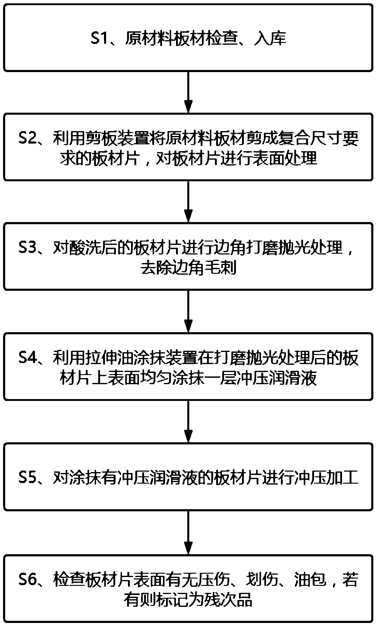
[0044] see figure 1 , a workpiece stamping process for processing electronic products, comprising the following steps:

[0045] S1. Inspection and storage of raw materials and plates;

[0046] S2. Use the shearing device to cut the raw material sheet into a sheet with a composite size requirement, and perform surface treatment on the sheet;

[0047] In S2, surface treatment includes the following steps:

[0048] S21. Pickling treatment: put the sheet into the pickling tank, add pickling liquid into the pickling tank, pickle at 30°C for 120-150min, and clean the sheet after the pickling;

[0049] S22. Passivation treatment: put the pickled sheet into a passivation tank, add a passivation solution to the passivation tank, and passivate the sheet at 20°C for 30 minutes;

[0050] S23. Cleaning and drying: the passivation-treated sheet is rinsed three times under a high-pressure water gun, and dried to complete the surface treatment.

[0051] Wherein, the pickling solution incl...

Embodiment 2

[0064] see figure 1 , a workpiece stamping process for processing electronic products, comprising the following steps:

[0065] S1. Inspection and storage of raw materials and plates;

[0066] S2. Use the shearing device to cut the raw material sheet into a sheet with a composite size requirement, and perform surface treatment on the sheet;

[0067] In S2, surface treatment includes the following steps:

[0068] S21. Pickling treatment: put the sheet into the pickling tank, add pickling liquid into the pickling tank, pickle at 35°C for 120-150min, and clean the sheet after the pickling;

[0069] S22. Passivation treatment: put the pickled sheet into a passivation tank, add a passivation solution to the passivation tank, and passivate the sheet at 25°C for 40 minutes;

[0070] S23. Cleaning and drying: wash the passivated sheet under a high-pressure water gun for 4 times, and dry to complete the surface treatment.

[0071] Wherein, the pickling solution includes the followi...


PUM


Abstract

The invention discloses a workpiece stamping process for electronic product machining, and belongs to the technical field of electronic product production. The workpiece stamping process for electronic product machining comprises the procedures of raw material plate inspection, storage, plate shearing treatment and surface treatment, grinding and polishing treatment, surface lubricating treatment,stamping machining, final inspection and the like. The workpiece stamping process for electronic product machining comprises the procedures of surface treatment, grinding and polishing treatment, lubricating and smearing treatment, stamping treatment and the like, the technological process is simple, and operation is easy; and the yield of stamping can be effectively increased, the stamping efficiency can be improved, the production cost is reduced, time is saved, and the workpiece stamping process is suitable for large-scale industrial production.

Description

technical field [0001] The invention relates to the technical field of electronic product processing, and more specifically, relates to a workpiece stamping process for electronic product processing. Background technique [0002] Electronic products are related products based on electric energy, mainly including: watches, smart phones, telephones, televisions, DVD players, video recorders, camcorders, radios, tape recorders, combination speakers, CD players, computers, game consoles, mobile communication products, etc. Because the early products were mainly based on electronic tubes, they were named electronic products. [0003] Stamping processing is a production technology that uses the power of conventional or special stamping equipment to directly subject the sheet to deformation force and deform in the mold, so as to obtain product parts of a certain shape, size and performance. Sheet metal, mold and equipment are the three elements of stamping processing. According ...

Claims


Application Information

Patent Timeline
Patent Type & Authority Applications(China)
IPC IPC(8): B23P15/00B21D22/02B21D37/16B21D37/18B24B1/00B24B9/04C23G1/02C23C22/44C10M173/02C10N30/06C10N40/24
CPCB21D22/02B21D37/16B21D37/18B23P15/00B24B1/00B24B9/04C10M173/02C10M2201/041C10M2207/021C10M2207/022C10M2207/281C10M2209/104C23C22/44C23G1/02C10M2209/108
Inventor 窦进军
Owner 昆山久茂电子科技有限公司
Why Eureka
Try Eureka