Semiconductor structure and forming method thereof

A semiconductor and auxiliary layer technology, used in semiconductor devices, semiconductor/solid-state device manufacturing, electrical components, etc., can solve problems such as poor flatness, polysilicon surface depression, etc., and achieve the effect of good flatness and high quality

Pending Publication Date: 2020-08-25
NEXCHIP SEMICON CO LTD
View PDF3 Cites 2 Cited by
  • Summary
  • Abstract
  • Description
  • Claims
  • Application Information

AI Technical Summary

Problems solved by technology

For example, in a method for forming isolated polysilicon units on a substrate, isolation structures higher than the surface of the substrate are first formed on the substrate, and then an oxide layer is formed on the substrate between the isolation structures and filled with polysilicon, and then using CMP removes the part of the polysilicon material higher than the top surface of the isolation structure, but the surface of the polysilicon obtained after CMP often has depressions and poor flatness, and the existing solutions cannot meet the requirements of high efficiency and economy

Method used


Image

  • Semiconductor structure and forming method thereof
  • Semiconductor structure and forming method thereof
  • Semiconductor structure and forming method thereof

Examples


Embodiment Construction

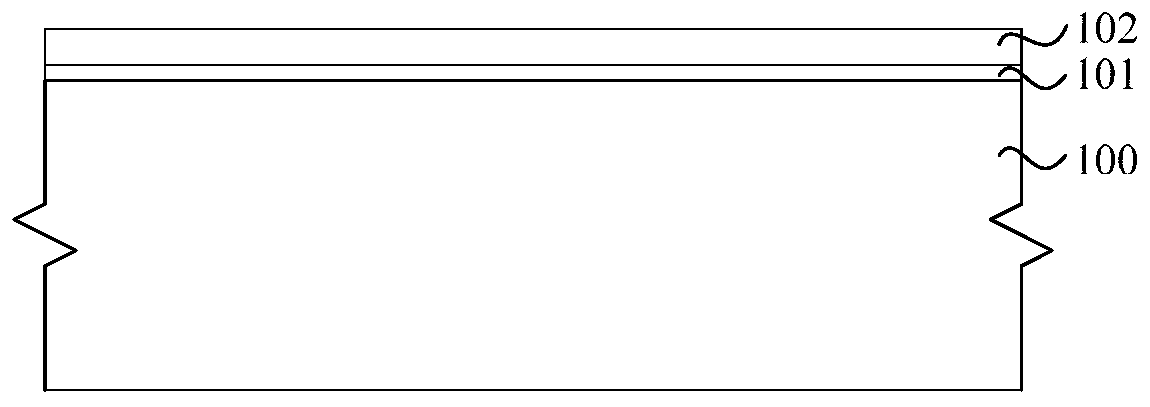
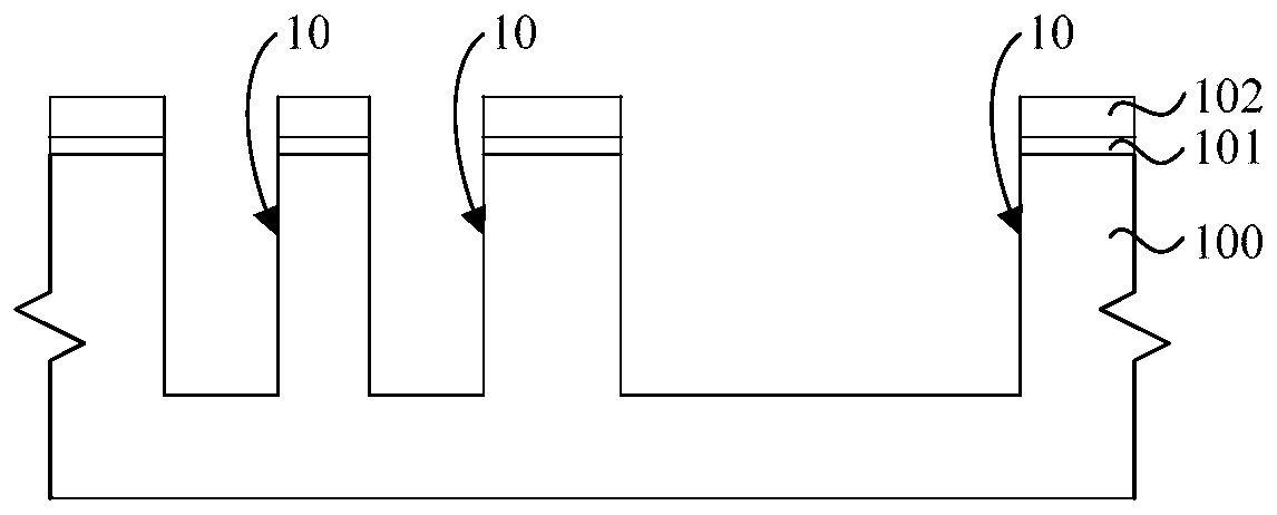
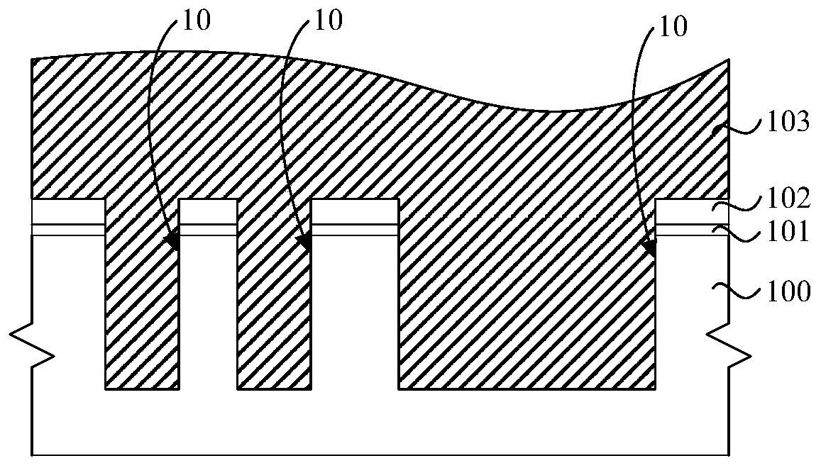
[0041]The semiconductor structure and its manufacturing method of the present invention will be further described in detail below in conjunction with the accompanying drawings and specific embodiments. The advantages and features of the present invention will become clearer from the following description. It should be noted that the drawings are all in a very simplified form and use inaccurate scales, and are only used to facilitate and clearly illustrate the embodiments of the present invention, and the embodiments of the present invention should not be considered limited to those shown in the drawings to show the specific shape of the region. For the sake of clarity, in all the drawings used to help explain the embodiments of the present invention, in principle, the same components are marked with the same reference numerals, and repeated descriptions thereof are omitted. The terms "first", "second", etc. hereinafter are used to distinguish between similar elements, and are...


PUM


Abstract

The invention provides a semiconductor structure and a forming method thereof. The forming method comprises the following steps: before filling a first groove on a pretreatment substrate by using a filling material, forming an auxiliary layer covering the inner surface of the first groove; forming a first filling medium and carrying out back etching, wherein the upper surface of the obtained firstfilling medium is higher than the upper surface of the pretreatment substrate; and then forming a second filling medium and executing a second planarization process. Since the grinding amount of thefirst groove region is greater than that of the surrounding region, the first groove region is not easy to sink after the second planarization process is completed; the process of filling the first groove does not need to adopt a photoresist and an exposure process, so that implementation is convenient, and the cost is lower; and according to the semiconductor structure formed by the forming method, the surface with better flatness can be obtained, so that the quality is higher.

Description

technical field [0001] The invention relates to the technical field of semiconductors, in particular to a semiconductor structure and a forming method thereof. Background technique [0002] In the manufacture of integrated circuits, the method of forming STI (Shallow Trench Isolation, Shallow Trench Isolation) is mostly used for the isolation between individual devices fabricated on the substrate, such as different memory cells and different transistors. A commonly used method for making STI includes the following process: first form a pad oxide layer and a silicon nitride layer on the substrate; then sequentially etch the silicon nitride layer, the pad oxide layer, and the substrate in a selected area to form an isolation trench; Next, an isolation dielectric is deposited on the substrate and CMP (Chemical Mechanical Polishing, chemical mechanical polishing) is performed, so that the isolation dielectric filled in the isolation trench is substantially flush with the upper s...

Claims


Application Information

Patent Timeline
Patent Type & Authority Applications(China)
IPC IPC(8): H01L29/06H01L21/762H01L21/311
CPCH01L29/0649H01L21/76224H01L21/31051H01L21/31053H01L21/31056H01L21/76229H01L21/76264
Inventor 陈笋弘郑存闵李瑞珉项伟朱人伟
Owner NEXCHIP SEMICON CO LTD
Why Eureka
Try Eureka