Supercharge Your Innovation With Domain-Expert AI Agents!

Random nanowire network topology analysis and electrical property simulation method

A technology of electrical properties and simulation methods, which is applied in the field of random nanowire network topology analysis and electrical property simulation, and can solve the problems of neglecting the resistance of nanowire segments, seldom judging the full conduction state, and many studies on seepage conduction.

Pending Publication Date: 2020-08-28
SOUTHEAST UNIV
View PDF4 Cites 3 Cited by
  • Summary
  • Abstract
  • Description
  • Claims
  • Application Information

AI Technical Summary

Problems solved by technology

Junction-dominated assumption (JDA) provides a simple calculation method for the square resistance of random nanowire networks, but often ignores the segment resistance of nanowires. When the junction resistance between nanowires is properly welded After the process is reduced to tens of ohms, it is impossible to accurately estimate the actual square resistance of the random nanowire network
[0006] For example, the geometric topology of the nanowire network cannot be intuitively reflected and well described in mathematical language in the simulation model. There are many studies on its percolation and conduction, and there are few judgments on the full conduction state.

Method used


Image

  • Random nanowire network topology analysis and electrical property simulation method
  • Random nanowire network topology analysis and electrical property simulation method

Examples


Embodiment Construction

[0023] In order to make the object, technical solution and advantages of the present invention clearer, the present invention will be further described in detail below in conjunction with specific embodiments.

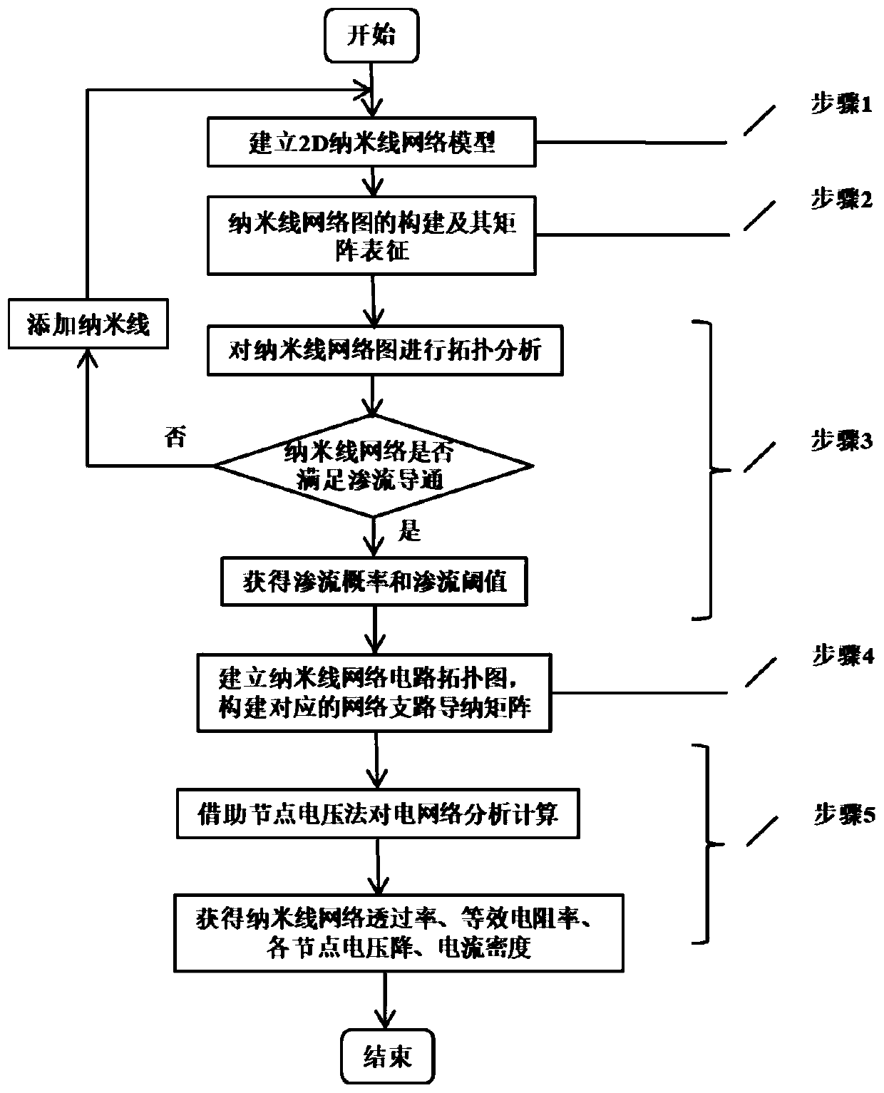
[0024] The invention provides a random nanowire network topology analysis and electrical property simulation method, including:

[0025] Step 1, establish a random nanowire network microstructure model:

[0026] Select the model according to the composition form of the random nanowire network: use the 2D model for the simulation of the random nanowire network applied to the two-dimensional film materials such as transparent conductive films; use the 3D model for the simulation of the random nanowire network applied to the three-dimensional materials such as conductive composite materials Model.

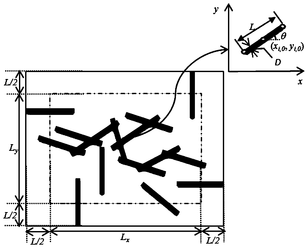
[0027] a. Establish a two-dimensional random nanowire network model, such as figure 2 shown; initially create an empty size (L x +L)×(L y +L), and then add straight penet...


PUM


Abstract

The invention discloses a random nanowire network topology analysis and electrical property simulation method. The method comprises the following steps: 1, constructing a random nanowire network microcosmic model; 2, describing the random nanowire network microcosmic model by utilizing a graph theory thought and a double-node model to obtain matrix representation of a graph; 3, performing topologyanalysis on the random nanowire network diagram; 4, establishing a random nanowire network circuit topological graph, and constructing a corresponding network branch admittance matrix; and 5, analyzing and calculating the electrical network by means of a node voltage method. The invention provides a more reliable and perfect random nanowire network topology analysis and electrical property simulation method. In consideration of basic physical quantities such as segment resistance, junction resistance, tunnel effect junction resistance and the like, topological analysis can be performed on therandom nanowire network, and a systematic and automatic method is adopted to construct and solve a circuit equation, so that simulation and emulation of electrical properties of the random nanowire network are realized through a computer.

Description

technical field [0001] The invention belongs to the technical field of design and analysis of advanced nanometer materials, in particular to a random nanowire network topology analysis and electrical property simulation method. Background technique [0002] Nanowires (tubes) with one-dimensional morphology have been extensively studied due to their unique structures and excellent physical properties. However, the construction and application of single nanowires in nanodevices is not ideal. In contrast, random nanowire networks composed of nanowire assemblies (such as carbon nanotubes, silver nanowires, copper nanowires, gold nanowires, and metal alloy nanowire networks) have good optoelectronic performance, flexible mechanical The advantages of responsiveness, low cost, and adaptability to large-scale production have attracted people's attention, and have very broad application prospects in the fields of transparent conductive electrodes, flexible sensing, touch, and displa...

Claims


Application Information

Patent Timeline
IPC IPC(8): G06F30/367G06F30/18G06F17/16
CPCG06F30/367G06F30/18G06F17/16G06F2111/10
Inventor 赵志伟翁正进方勇吴锦东江和龙
Owner SOUTHEAST UNIV
Features
  • R&D
  • Intellectual Property
  • Life Sciences
  • Materials
  • Tech Scout
  • Unparalleled Data Quality
  • Higher Quality Content
  • 60% Fewer Hallucinations
Learn More