
Deep-hole processing device for semiconductor material

A processing device and semiconductor technology, applied in metal processing equipment, metal processing mechanical parts, manufacturing tools, etc., can solve the problems of damage to the drill, loose drill, cracking of the installation base, etc., to reduce rigid meshing friction, prolong the Long service life and good shock absorption effect

Inactive Publication Date: 2020-09-04
郭志锋
View PDF0 Cites 1 Cited by
  • Summary
  • Abstract
  • Description
  • Claims
  • Application Information

AI Technical Summary

Problems solved by technology

[0002] Semiconductor material is a kind of electronic material with semiconductor properties that can be used to make semiconductor devices and integrated circuits. When deep hole processing is carried out, semiconductor materials are mostly processed by deep hole drilling machines. Due to the limitation of the diameter of the tool holder, the diameter is small and the length Large, resulting in poor rigidity, low strength, easy to generate vibration during deep hole processing, which easily affects the straightness of the deep hole, making the deep hole processing rough, and the vibration is easy to cause damage to the drill, so the drill needs to be replaced. Most of the existing drills are installed through screw thread rotation connection. Since the drill is in a rotating state during deep hole machining, if the rotation direction is the same as the thread rotation direction, it is easy to make the drill loose. If the rotation direction is opposite to the thread rotation direction , it is easy to make the drill bit rotate too much and cause the installation base to crack

Method used


Image

  • Deep-hole processing device for semiconductor material
  • Deep-hole processing device for semiconductor material
  • Deep-hole processing device for semiconductor material

Examples


Embodiment 1

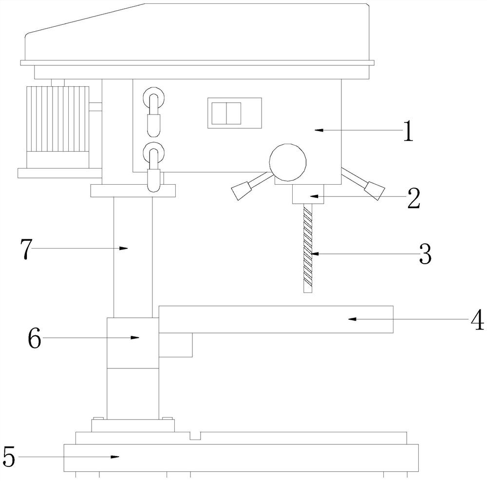
[0037] see Figure 1-5 , the present invention provides a technical scheme of a semiconductor material deep hole processing device: its structure includes an organic body 1, a mounting head 2, a deep hole drill 3, a workbench 4, a base 5, a nut lifting seat 6, a screw rod 7, and the base 5 Connected with the body 1 by a screw 7, the screw 7 is connected with a nut lifting seat 6, and the nut lifting seat 6 is connected to the workbench 4, and the top of the workbench 4 is provided with a deep hole drill 3, and the deep hole drill 3 is connected to the installation head 2, and the installation head 2 is movably connected with the body 1.

[0038]The deep hole drill bit 3 includes a cutter body R1, an inclined circular groove R2, a card track R3, and a positioning groove R4. The top surface of the cutter body R1 is provided with a positioning groove R4, and the cutter body R1 is also provided with a The card track R3, three inclined circular grooves R2 arranged equidistantly ar...

Embodiment 2

[0041] see Figure 6-7 , the base Q1 includes a base body Q11, an inclined hole Q12, an installation slot Q13, an annular cavity Q14, a through hole Q15, and a positioning column Q16, and the center of the base body Q11 is provided with a cylindrical installation slot Q13, and the installation The slot Q13 is provided with a positioning column Q16 which is an integral structure with the base body Q11, and the base body Q11 is also provided with an annular cavity Q14, and the annular cavity Q14 communicates with the through hole Q15 and the inclined hole Q12, and the inclined hole Q12, through The hole Q15 is arranged on the base body Q11, the rotating assembly Q3 and the power gear set Q5 are located in the annular chamber Q14, the regular triangular hole R41 is matched with the regular triangular prism of the positioning column Q16, and the isosceles triangular hole R42 is matched with the regular triangular prism of the positioning column Q16. The isosceles triangular prism ...


PUM


Abstract

The invention discloses a deep-hole processing device for a semiconductor material. The deep-hole processing device for the semiconductor material structurally comprises a machine body, an installation head, a deep-hole drilling bit, a workbench, a base, a nut lifting seat and a screw, wherein the base is connected with the machine body through the screw; the nut lifting seat is connected to the screw; the nut lifting seat is connected to the workbench; and the deep-hole drilling bit is arranged above the workbench. Compared with the prior art, the deep-hole processing device for the semiconductor material has the following beneficial effects: the deep-hole processing device for the semiconductor material has a function of shock absorption, and is capable of reducing vibration generated during deep-hole processing and avoiding influence on the straightness of the deep-hole processing, conducive to increasing the accuracy of the deep-hole processing, and capable of rapidly changing a drilling tool; and the drilling tool is installed in a clamping manner, stable clamping is achieved, the loosening of a tool body due to the influence of rotation during the deep-hole processing is effectively prevented, and the cracking of a pedestal can also be avoided.

Description

technical field [0001] The invention relates to the technical field of semiconductors, in particular to a deep hole processing device for semiconductor materials. Background technique [0002] Semiconductor material is a kind of electronic material with semiconductor properties that can be used to make semiconductor devices and integrated circuits. When deep hole processing is carried out, semiconductor materials are mostly processed by deep hole drilling machines. Due to the limitation of the diameter of the tool holder, the diameter is small and the length Large, resulting in poor rigidity, low strength, easy to generate vibration during deep hole processing, which easily affects the straightness of the deep hole, making the deep hole processing rough, and the vibration is easy to cause damage to the drill, so the drill needs to be replaced. Most of the existing drills are installed through screw thread rotation connection. Since the drill is in a rotating state during dee...

Claims


Application Information

Patent Timeline
IPC IPC(8): B23B41/02B23Q11/00
CPCB23B41/02B23B2250/16B23Q11/0032
Inventor 郭志锋
Owner 郭志锋
Learn More