Semiconductor device and electric contact structure and manufacturing method thereof

A manufacturing method and electrical contact technology, which are applied in the fields of semiconductor/solid-state device manufacturing, semiconductor devices, semiconductor/solid-state device components, etc., can solve problems such as abnormal electrical structure of contact plugs, and achieve the effect of avoiding abnormality or collapse.

Pending Publication Date: 2020-09-08
FUJIAN JINHUA INTEGRATED CIRCUIT CO LTD
View PDF0 Cites 6 Cited by
  • Summary
  • Abstract
  • Description
  • Claims
  • Application Information

AI Technical Summary

Problems solved by technology

[0004] The object of the present invention is to provide a semiconductor device and its electrical contact structure and manufacturing method, to solve the problem of the core area boundary caused by the optical proximity effect and the dense / sparse effect of circuit patterns in existing semiconductor devices such as dynamic random access memories. Problems such as abnormal electrical structure connected to the outermost contact plug to improve device performance

Method used


Image

  • Semiconductor device and electric contact structure and manufacturing method thereof
  • Semiconductor device and electric contact structure and manufacturing method thereof
  • Semiconductor device and electric contact structure and manufacturing method thereof

Examples


Embodiment Construction

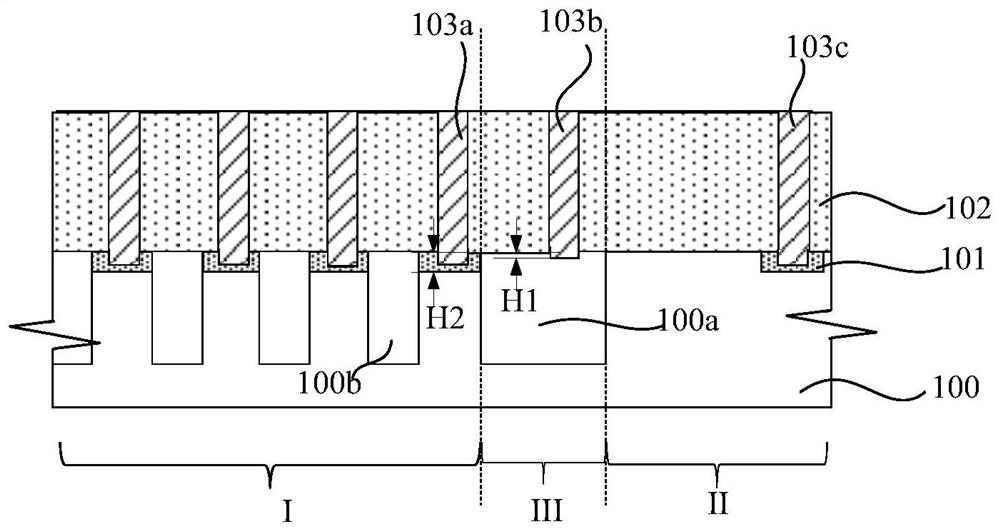
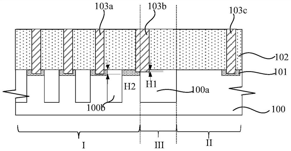
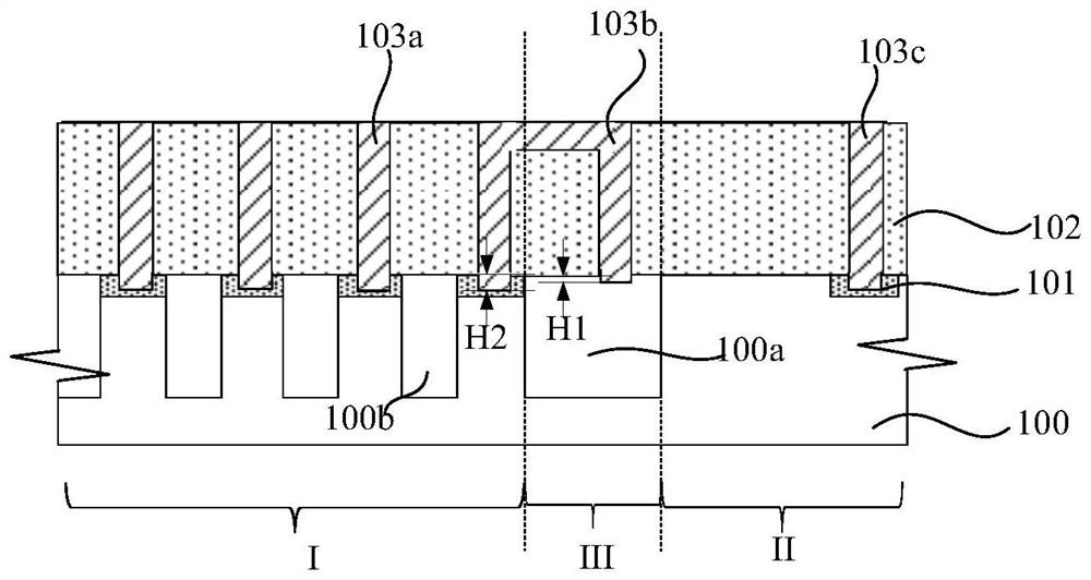
[0025] The memory and its forming method proposed by the present invention will be further described in detail below with reference to the drawings and specific embodiments. The advantages and features of the present invention will become clearer from the following description. It should be noted that all the drawings are in a very simplified form and use imprecise scales, and are only used to facilitate and clearly assist the purpose of illustrating the embodiments of the present invention.

[0026] Figure 1A is a schematic cross-sectional view showing an electrical contact structure of a semiconductor device according to an embodiment of the present invention. Please refer to Figure 1A An electrical contact structure of a semiconductor device provided by an embodiment of the present invention includes: a substrate 100 and a plurality of contact plugs 103a, 103b. Wherein, the substrate 100 has a core area I and a peripheral area II and an isolation structure 100a located...


PUM


Abstract

The invention provides a semiconductor device and an electric contact structure and a manufacturing method thereof. At least a first contact plug closest to a peripheral region in a core region is formed above an isolation structure at the junction of the core region and the peripheral region and is in contact with the isolation structure; the bottom of the first contact plug can be completely overlapped on the isolation structure; or, a part of the bottom is overlapped with the isolation structure; the bottom of the other part is overlapped with the active region close to the core region of the isolation structure; and even the top of the first contact plug is at least connected with the top of the contact plug close to the upper part of the active region of the core region of the isolation structure, so that the electrical structure originally formed on the outermost side of the boundary of the core region can be at least partially formed above the isolation structure at the junction, the consistency of the electrical structure above the contact plug in the core region is ensured, and the performance of the electrical structure on the boundary of the core region is ensured.

Description

technical field [0001] The invention relates to the technical field of semiconductors, in particular to a semiconductor device and its electrical contact structure and manufacturing method. Background technique [0002] Various techniques have been used to integrate more circuit patterns in a limited area of ​​a semiconductor substrate or wafer. Due to the difference in circuit pattern spacing, integrated circuits are generally divided into device-dense areas (Dense), device-sparse areas (ISO) and device-isolated areas. It is an area where the device density is low (that is, the devices are relatively sparse), and the device isolated area is an area where relatively sparse areas and dense areas are set separately. As the critical dimensions of semiconductor devices continue to decrease, the density of circuit patterns and / or device heights continue to increase, subject to the resolution limit of the optical exposure tool and the density difference between device-dense regio...

Claims


Application Information

Patent Timeline
Patent Type & Authority Applications(China)
IPC IPC(8): H01L27/108H01L23/48H01L21/768H01L21/8242
CPCH01L23/481H01L21/76895H10B12/34H10B12/488H10B12/485H10B12/0335H10B12/482
Inventor 童宇诚赖惠先
Owner FUJIAN JINHUA INTEGRATED CIRCUIT CO LTD
Why Eureka
Try Eureka