Method for optimizing self-alignment process of silicon carbide MOSFET

A self-alignment process, silicon carbide technology, applied in the direction of electrical components, semiconductor/solid-state device manufacturing, circuits, etc., can solve the problem of increasing the manufacturing cost of semiconductor devices

Pending Publication Date: 2020-09-11
SHENZHEN BASIC SEMICON LTD
View PDF6 Cites 0 Cited by
  • Summary
  • Abstract
  • Description
  • Claims
  • Application Information

AI Technical Summary

Problems solved by technology

[0003] From the perspective of cost, each additional layer of photomask will increase the manufacturing cost of semiconductor devices; from the perspective of processing cycle, each additional layer of photomask will increase the processing time by about 7 days

Method used


Image

  • Method for optimizing self-alignment process of silicon carbide MOSFET
  • Method for optimizing self-alignment process of silicon carbide MOSFET
  • Method for optimizing self-alignment process of silicon carbide MOSFET

Examples


Embodiment Construction

[0045] In order to make the object, technical solution and advantages of the present invention clearer, the present invention will be further described in detail below in conjunction with the accompanying drawings and specific embodiments. It should be understood that the specific embodiments described here are only used to explain the present invention, not to limit the present invention.

[0046] The invention provides a method for optimizing the silicon carbide MOSFET self-alignment process. Please refer to Figure 2 to Figure 10 According to a preferred embodiment of the present invention, the method for optimizing the silicon carbide MOSFET self-alignment process includes the following steps:

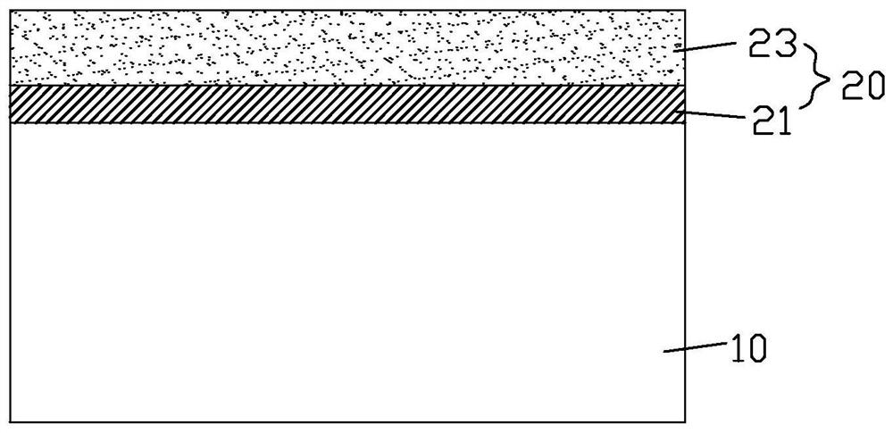
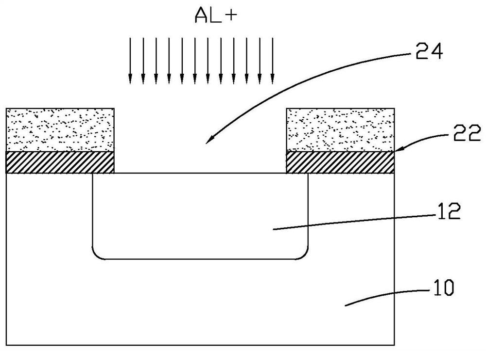
[0047] S1, such as figure 2 As shown, a silicon carbide substrate 10 is provided, and a first mask layer 20 is deposited on the surface of the silicon carbide substrate 10 . In this embodiment, the first mask layer 20 includes a first SiO 2 Thin film layer 21 and polysilicon l...


PUM


Abstract

The invention discloses a method for optimizing a self-alignment process of a silicon carbide MOSFET, which comprises the following steps of: etching a first ion implantation region only by using a layer of P-well photomask to form a P well; forming a second ion implantation region in the first ion implantation region through deposition, etching and other processes so as to form an NPlus region and a Plus region of the laminated layer; and finally, etching a groove of which the depth is greater than the depth of the NPlus region and less than the depth of the Plus region so as to form a corresponding PN junction on the silicon carbide substrate. According to the method, only one layer of photomask is used in the process of forming the P trap, the NPlus region and the Plus region, so that the processes of twice thin film deposition, gluing, exposure, development, photoresist removal and the like are reduced, the processing period is greatly shortened, and the manufacturing cost is reduced.

Description

technical field [0001] The invention relates to the field of semiconductor manufacturing, in particular to a method for optimizing a silicon carbide MOSFET self-alignment process. Background technique [0002] The traditional self-alignment process of silicon carbide MOSFET usually requires Pwell, NPlus, PPlus three-layer mask, repeated thin film deposition, photolithography, etching, ion implantation and other processes, and finally forms a corresponding PN junction on silicon carbide. Such as figure 1 shown. [0003] From the perspective of cost, each additional layer of photomask will increase the manufacturing cost of semiconductor devices; from the perspective of processing cycle, each additional layer of photomask will increase the processing time by about 7 days. Therefore, it is desired to provide a method for optimizing the self-aligned trench etching process to optimize the above-mentioned self-aligned process, so as to shorten the processing cycle and reduce the...

Claims


Application Information

Patent Timeline
Patent Type & Authority Applications(China)
IPC IPC(8): H01L21/336H01L29/16
CPCH01L29/66068H01L29/1608
Inventor 郝建勇孙军张振中和巍巍
Owner SHENZHEN BASIC SEMICON LTD
Why Eureka
Try Eureka