Automatic elimination circuit for input offset voltage of operational amplifier

A technology of operational amplifier and offset voltage, which is applied in the field of automatic elimination circuit, and can solve the problem that the input offset voltage of the amplifier cannot be fully eliminated.

Active Publication Date: 2020-09-15
XIDIAN UNIV
View PDF8 Cites 0 Cited by
  • Summary
  • Abstract
  • Description
  • Claims
  • Application Information

AI Technical Summary

Problems solved by technology

In the process of circuit design, it is usually taken to maximize the matching of transistors in the layout layout, or to optimize the size of transistors to minimize the input offset voltage of the operational amplifier, but in general, the input offset voltage of the amplifier is between cannot be adequately eliminated after taking the above measures

Method used


Image

  • Automatic elimination circuit for input offset voltage of operational amplifier
  • Automatic elimination circuit for input offset voltage of operational amplifier
  • Automatic elimination circuit for input offset voltage of operational amplifier

Examples


Embodiment 1

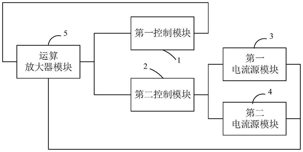
[0051] See figure 1 , figure 1 It is a module schematic diagram of an automatic elimination circuit of an operational amplifier input offset voltage provided by an embodiment of the present invention. As shown in the figure, the automatic elimination circuit of an operational amplifier input offset voltage in this embodiment includes a first control module 1, a second Control module 2, the first current source module 3, the second current source module 4 and operational amplifier module 5, wherein, the first control module 1 produces the first control signal according to the output signal of operational amplifier module 5; The second control module 2 according to The output signal of the operational amplifier module 5 generates a second control signal; the first current source module 3 and the second current source module 4 generate a current signal according to the second control signal; the operational amplifier module 5 realizes the input offset voltage according to the cur...

Embodiment 2

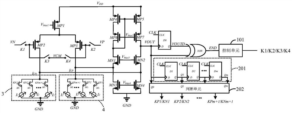
[0063] This embodiment specifically describes the working principle of the automatic elimination circuit for the input offset voltage of the operational amplifier in Embodiment 1. The automatic elimination circuit for the input offset voltage of the operational amplifier in this embodiment includes Offset-Cancelling (OC) mode and In the normal-operation (Normal-Operation, NO) mode, before entering the NO mode, it is first necessary to complete the background elimination of the input offset voltage of the operational amplifier module 5 in the OC mode.

[0064] In the OC mode, the first switch K1 and the second switch K2 are turned off, and at the same time, the third switch K3 and the fourth switch K4 are turned on, and the differential input pair controls the gate voltage of the second PMOS transistor MP2 and the third PMOS transistor MP3 Connect to common mode input voltage terminal VCM. At this time, the operational amplifier module 5 works in an open-loop circuit state. Du...


PUM


Abstract

The invention relates to an automatic elimination circuit for input offset voltage of an operational amplifier, which comprises a first control module, a second control module, a first current sourcemodule, a second current source module and an operational amplifier module, wherein the first control module generates a first control signal according to an output signal of the operational amplifiermodule; the second control module generates a second control signal according to the output signal of the operational amplifier module; the first current source module and the second current source module generate current signals according to the second control signal; the operational amplifier module achieves elimination of input offset voltage according to the current signal and achieves switching between an offset elimination mode and a working mode according to the first control signal. The automatic elimination circuit provided by the invention does not influence the working state of theoperational amplifier while eliminating the offset voltage.

Description

technical field [0001] The invention belongs to the technical field of integrated circuits, and in particular relates to an automatic elimination circuit of an operational amplifier input offset voltage. Background technique [0002] As the key circuit unit of analog integrated circuits, operational amplifiers are widely used in A / D (analog / digital) converters and D / A (digital / analog) converters to realize functions such as circuit driving and analog-to-digital conversion. In some application fields such as test and measurement, the static parameters of gain error and offset error of A / D or D / A converter are very important performance indicators. For example, the time domain interleaving analog-to-digital converter achieves the design goal of high sampling rate of the converter by sampling the input signal through each channel converter in turn in the time domain, but the mismatch between the gain error and offset error of each channel converter Harmonics will appear in the...

Claims


Application Information

Patent Timeline
Patent Type & Authority Applications(China)
IPC IPC(8): H03F1/30
CPCH03F1/301
Inventor 梁宇华朱樟明杨银堂丁瑞雪刘术彬
Owner XIDIAN UNIV
Why Eureka
Try Eureka