Gallium nitride power device with grid high voltage resistance and low electric leakage

A power device, gallium nitride technology, applied in electrical components, semiconductor devices, circuits, etc., can solve the problems of low forward threshold voltage of devices, increased gate leakage, gate leakage, etc., to improve practicability and safety. Effect

Pending Publication Date: 2021-12-10
SOUTHEAST UNIV +1
View PDF3 Cites 0 Cited by
  • Summary
  • Abstract
  • Description
  • Claims
  • Application Information

AI Technical Summary

Problems solved by technology

[0005] The present invention proposes a novel gallium nitride power device structure for the problems of increased gate leakage under high voltage and low device forward threshold voltage in P-type gallium nitride gate high electron mobility transistor power devices. This structure can It is a good solution to the problems of gate leakage and threshold voltage of GaN power devices, thereby improving the practicability and safety of the devices

Method used


Image

  • Gallium nitride power device with grid high voltage resistance and low electric leakage
  • Gallium nitride power device with grid high voltage resistance and low electric leakage
  • Gallium nitride power device with grid high voltage resistance and low electric leakage

Examples


Embodiment Construction

[0022] Below in conjunction with accompanying drawing, the present invention is described in detail:

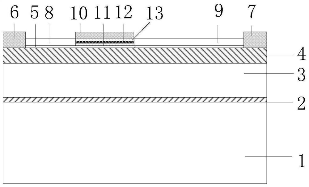
[0023] The gallium nitride power device with low gate leakage and high threshold voltage according to the present invention comprises: a P-type silicon substrate 1, an aluminum nitride buffer layer 2 is provided on the P-type silicon substrate 1, and the aluminum nitride buffer layer 2 is provided. An AlGaN buffer layer 3 is provided above the layer 2, a GaN buffer layer 4 is provided above the AlGaN buffer layer 3, and an AlGaN barrier layer 5 and source electrodes 6 at both ends are provided above the GaN buffer layer 4. and drain 7, there is metal above source 6 and drain 7 as source 6 and drain 7 respectively connecting both ends of AlGaN barrier layer 5 to the peripheral input / output, source 6 metal and AlGaN An ohmic contact is formed at the left end of the barrier layer 5 , an ohmic contact is formed between the drain 7 and the right end of the AlGaN barrier layer 5 , ...


PUM


Abstract

A gallium nitride power device with a high-voltage-resistance grid and low electric leakage comprises a P-type silicon substrate, an aluminum nitride buffer layer arranged on the P-type silicon substrate, an aluminum-gallium-nitrogen buffer layer arranged on the aluminum nitride buffer layer, a gallium nitride buffer layer arranged on the aluminum-gallium-nitrogen buffer layer, an aluminum-gallium-nitrogen barrier layer arranged on the gallium nitride buffer layer, a source electrode and a drain electrode, metal is arranged above the source electrode and the drain electrode to be used as the source electrode and the drain electrode to be connected with input and output from the two ends of the aluminum-gallium-nitrogen barrier layer to the periphery, ohmic contact is formed between the source electrode metal and the left end of the aluminum-gallium-nitrogen barrier layer, ohmic contact is formed between the drain electrode and the right end of the aluminum-gallium-nitrogen barrier layer, three P-type gallium nitride layers with different doping concentrations are stacked above the aluminum-gallium-nitrogen barrier layer, gate metal is arranged above the P-type gallium nitride layer to connect the P-type gallium nitride layer to input and output at the periphery of the structure, the gate metal and the P-type gallium nitride layer form Schottky contact, the P-type gallium nitride layer and the gate are relatively close to the source electrode and relatively far away from the drain electrode between the source electrode and the drain electrode, a nitride passivation layer is arranged between the drain electrode and the P-type gallium nitride above the aluminum gallium nitride barrier layer, and a nitride passivation layer is arranged between the source electrode and the P-type gallium nitride.

Description

technical field [0001] The present invention mainly relates to the technical field of high-voltage power semiconductor devices, in particular, to a gallium nitride power device that can protect the gate well, that is, maintain high gate voltage and low leakage. Background technique [0002] With the popularity of power electronics, semiconductor lighting, new generation mobile communications, smart grid, high-speed rail transit, new energy vehicles, consumer electronics and other fields, the rise of wireless charging, driverless cars, solid-state light sources, microwave radio frequency devices and other applications , which puts forward new demands on the performance of power devices. However, due to the influence of material characteristics, traditional silicon devices have reached the physical limit and can no longer meet emerging needs in terms of performance. Therefore, it is imperative to seek the next replacement driven by social needs. Compared with the first-genera...

Claims


Application Information

Patent Timeline
Patent Type & Authority Applications(China)
IPC IPC(8): H01L29/06H01L29/778
CPCH01L29/0619H01L29/0692H01L29/7781H01L29/0638
Inventor 张龙崔永久刘培港马杰骆敏王肖娜孙伟锋时龙兴
Owner SOUTHEAST UNIV
Why Eureka
Try Eureka