Three dimensional integrated circuit

An integrated circuit, three-dimensional technology, applied in the direction of circuits, electrical components, electrical solid devices, etc., to achieve the effect of increasing signal bandwidth, improving system functionality, and reducing layer separation

Pending Publication Date: 2020-09-18
SILICON GENERAL CORPORATION
View PDF4 Cites 3 Cited by
  • Summary
  • Abstract
  • Description
  • Claims
  • Application Information

AI Technical Summary

Problems solved by technology

Substrates can be processed at wafer level

Method used


Image

  • Three dimensional integrated circuit
  • Three dimensional integrated circuit
  • Three dimensional integrated circuit

Examples


Embodiment Construction

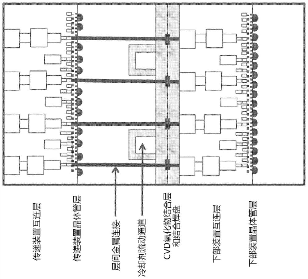
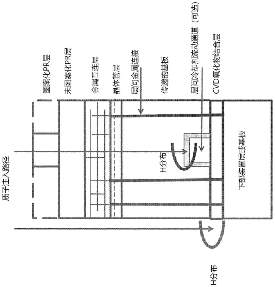
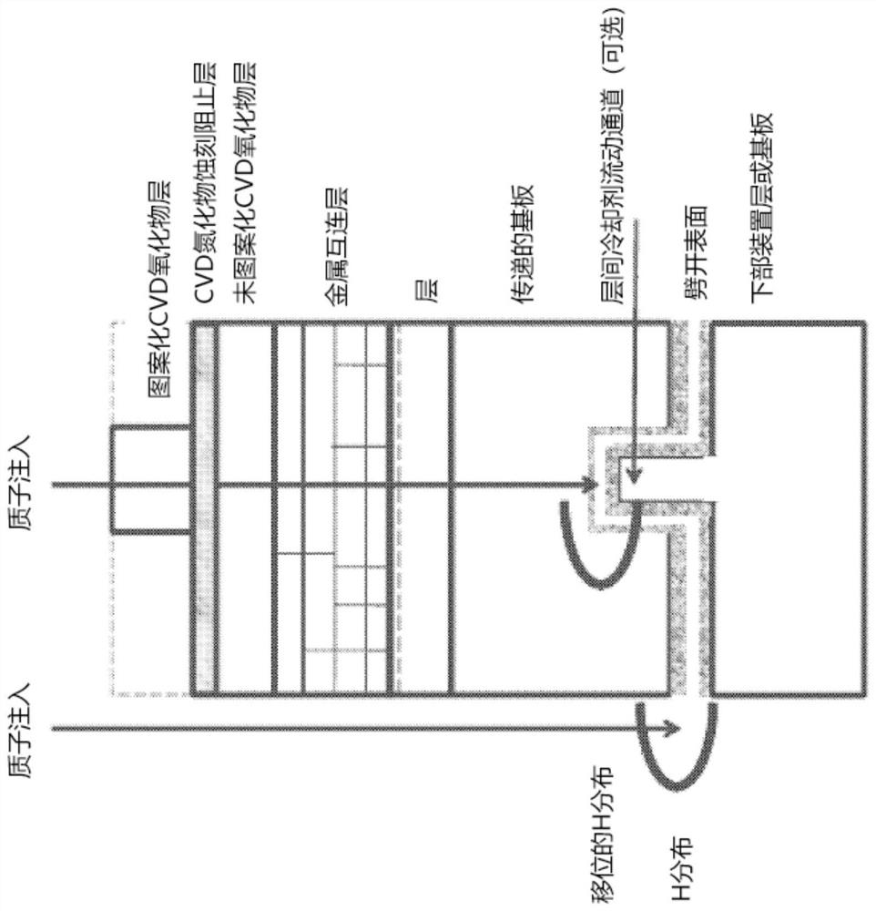
[0086] According to the present invention, techniques generally related to the fabrication of integrated circuit devices are provided. More specifically, the present invention provides a method and resulting devices for stacking and interconnecting three-dimensional (3-D) devices using heterogeneous and non-uniform layers (eg, fully fabricated integrated circuits). For example, an integrated circuit may include, among other things, memory means, processor means, digital signal processing means, application-specific means, controller means, communication means, and the like.

[0087] The embodiments build upon and extend the capabilities of two broad areas of technology, layer transfer methods for forming bonded stacks of homogeneous layers (e.g., forming silicon-on-insulator (SOI) wafers) and various methods currently in use and development, 3-D electronic device stacks are formed through the use of complex interposers and sparse arrays of metal vias for inter-device connectio...


PUM

PropertyMeasurementUnit
thicknessaaaaaaaaaa
lengthaaaaaaaaaa

Abstract

Implanting ions to form a cleave layer in a semiconductor device causes damage to sensitive materials such as high-K dielectrics. In a process for forming a cleave layer and repairing damage caused byion implantation, ions are implanted through a circuit layer of a substrate to form a cleave plane. The substrate is exposed to a hydrogen gas mixture for a first time at a first temperature to repair damage caused by the implanted ions. A cleaving process may then be performed, and the cleaved substrate may be stacked in a 3DIC structure. A stacked device is formed by bonding a die to a first substrate, the die having a smaller width than a width of the first substrate, depositing a planarization material over the die, planarizing the planarization material to form a planarized upper surface, and stacking a third substrate on the planarized upper surface.

Description

[0001] Cross References to Related Applications [0002] This application claims priority to U.S. Application Serial No. 16 / 057,747, filed August 7, 2018, which is a continuation-in-part of U.S. Application Serial No. 15 / 899,622, filed February 20, 2018 , U.S. Application No. 15 / 899,622 is a continuation-in-part of U.S. Application No. 15 / 829,442 filed December 1, 2017, and U.S. Application No. 15 / 829,442 is now U.S. Patent No. 10,049,915. Each of these applications is incorporated herein in its entirety. Background technique [0003] Semiconductor substrates in conventional chip stacks are typically thinned using a mechanical backgrinding process. Backgrinding places a high degree of mechanical stress on the device and can result in large thickness variations. Therefore, it is desirable to have other processes for separating substrates. [0004] One method of thinning a substrate is described in US Patent No. 6,316,333 (hereinafter "Bruel"). Bruel describes implanting ion...

Claims


Application Information

Patent Timeline
Patent Type & Authority Applications(China)
IPC IPC(8): H01L21/822
CPCH01L21/8221H01L2224/13101H01L2924/14H01L2224/29186H01L2224/08145H01L2224/80895H01L2224/83896H01L25/50H01L24/80H01L24/83H01L24/32H01L24/08H01L24/94H01L2224/80006H01L2224/83005H01L2221/68304H01L2224/32145H01L24/29H01L2224/0557H01L24/05H01L21/6835H01L2221/68368H01L23/473H01L25/18H01L25/074H01L25/0657H01L23/481H01L2224/80896H01L21/7806H01L21/2007H01L2924/014H01L2924/00014H01L2924/00012H01L23/50H01L24/18H01L21/187
Inventor T·E·鄺M·I·柯伦特
Owner SILICON GENERAL CORPORATION
Why Eureka
Try Eureka