Wide-angle wave absorbing structure design method based on additive manufacturing

A technology of additive manufacturing and design methods, applied in computer-aided design, design optimization/simulation, calculation, etc., can solve problems such as long production cycle, distortion of wave-absorbing structure performance, narrow absorption angle, etc., and achieve good impedance matching characteristics, The effect of lightweight design and strong imaginary part loss capability

Active Publication Date: 2020-09-22
XI AN JIAOTONG UNIV
View PDF7 Cites 3 Cited by
  • Summary
  • Abstract
  • Description
  • Claims
  • Application Information

AI Technical Summary

Problems solved by technology

However, the performance of existing absorbing structures will be distorted, degraded, or even become electromagnetic wave reflecting structures as the incident angle of electromagnetic waves increases.
The absorbing structure faces two key problems that need to be solved urgently: 1. Narrow absorption angle; 2. Distortion of absorption performance within a wide angle
[0004] The traditional honeycomb absorbing structure impregnates the absorbing agent through the paper honeycomb board, which cannot meet the design requirements of wide oblique incidence in terms of material and structure, and the absorption ability of wide oblique incidence angle is weak
The development of 3D printing technology provides new ideas for the design of absorbing structures in terms of materials and structures, but the existing design methods are limited by the processing technology, the production cycle is long and the variability is small, and the technology of 3D printing has not been fully utilized. Advantages to realize the design and manufacture of absorbing structures with wide oblique incident angles

Method used


Image

  • Wide-angle wave absorbing structure design method based on additive manufacturing
  • Wide-angle wave absorbing structure design method based on additive manufacturing
  • Wide-angle wave absorbing structure design method based on additive manufacturing

Examples


Embodiment Construction

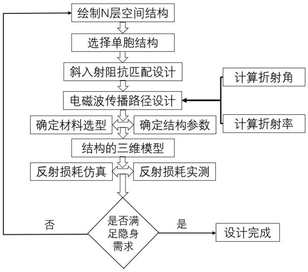
[0035] The method of the present invention will be described in detail below in conjunction with the accompanying drawings and embodiments.

[0036] refer to figure 1, a method for designing a wide-angle absorbing structure based on additive manufacturing, including the following steps:

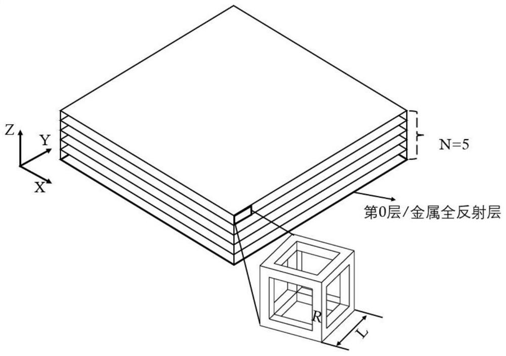
[0037] 1) Refer to figure 2 , according to the shape and size of the stealth target, its size is 180*180*20 millimeters (mm), the structure is divided into 5 layers, the thickness of each layer is 4mm, the bottom layer is a metal total reflection layer, the thickness is not counted, the first ~ 5 layers are impedance matching and loss absorbing layers;

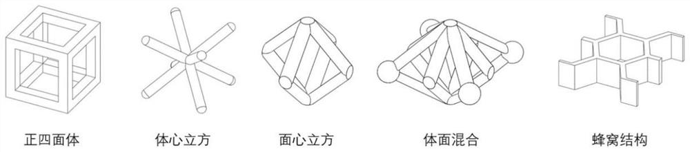
[0038] 2) Refer to image 3 , image 3 It is a schematic diagram of a unit cell structure. The unit cell structure includes a regular tetrahedron, a body-centered cubic, a face-centered cubic, a mixture of decent surfaces, and a honeycomb structure. In this embodiment, the regular tetrahedron structure is selected as the unit cell struct...


PUM


Abstract

A wide-angle wave absorbing structure design method based on additive manufacturing comprises the steps that a structure is divided into multiple layers according to the appearance and size of a stealth target, multiple layers of unit cell structures are selected, and the unit cell structures are periodically arrayed to form a multilayer structure; then multilayer oblique incidence impedance matching design is performed on the TE wave and the TM wave, an electromagnetic wave propagation path is designed and planned in the multilayer structure, and multilayer equivalent electromagnetic parameters are calculated; the design and control of the equivalent electromagnetic parameters are realized by controlling the variety and the proportion of an absorbent in a composite material and controlling the structural parameters of the unit cells; optimization is performed to obtain the types and proportions of the multilayer materials and the structural parameters of the unit cells; and modeling is performed, the reflection loss is calculated through simulation or the reflection loss is actually measured through 3D printing, and whether the design requirements are met or not is verified. According to the invention, the function of absorbing large electromagnetic waves with wide incident angles is realized, and the absorption angle can be actively designed, regulated and controlled.

Description

technical field [0001] The invention relates to the technical field of electromagnetic functional materials and structures, in particular to a method for designing a wide-angle absorbing structure based on additive manufacturing. Background technique [0002] The radar absorbing structure can reduce the detection distance by absorbing and scattering the detection signal of the enemy radar, which is an important technical way to realize radar wave stealth. However, the performance of the existing absorbing structure will be distorted, degraded, or even become an electromagnetic wave reflecting structure as the incident angle of the electromagnetic wave increases. The absorbing structure faces two key problems that need to be solved urgently: 1. The absorption angle is narrow; 2. The absorption performance is distorted in a wide angle. [0003] The radar absorbing structure requires multi-layer oblique incidence impedance matching and electromagnetic wave propagation path des...

Claims


Application Information

Patent Timeline
Patent Type & Authority Applications(China)
IPC IPC(8): G06F30/17G06F30/20G06T17/00G06F113/10
CPCG06F30/17G06F30/20G06T17/00G06F2113/10
Inventor 李涤尘尹义发张志坤曹毅杨东
Owner XI AN JIAOTONG UNIV
Why Eureka
Try Eureka