Wave-absorbing material and manufacturing method thereof
A technology of a wave absorbing material and a manufacturing method, applied in the field of wave absorbing material and its manufacturing, can solve the problems of poor impedance matching and corrosion resistance of carbonyl iron powder, large volume duty ratio of absorber, poor low frequency absorption performance, etc. The effect of improving the absorbing performance, extending the effective transmission path and improving the stability
- Summary
- Abstract
- Description
- Claims
- Application Information
AI Technical Summary
Problems solved by technology
Method used
Image
Examples
preparation example Construction
[0039]In the traditional preparation method of forming composite absorbing materials, the core material is usually placed in a solution for chemical reaction or physical adsorption to form a composite absorbing material. By controlling the parameters such as solution concentration and reaction time, it is roughly estimated The thickness of the material layer, the traditional process is difficult to accurately control the thickness of each material layer, especially when the thickness of the material layer is required to be small, it is more difficult to control the thickness of the material layer. In order to form a capacitor-like structure, the embodiment of the present invention needs to precisely control the thickness of the gap layer at 1-10nm, so a more accurate and easy-to-control atomic layer deposition technique is used to form a sacrificial layer, and the sacrificial layer is further removed to form a gap layer, so that the atoms Layer deposition technology can precise...
Embodiment 1
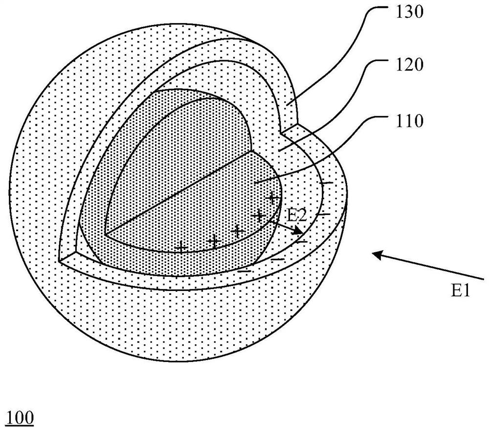
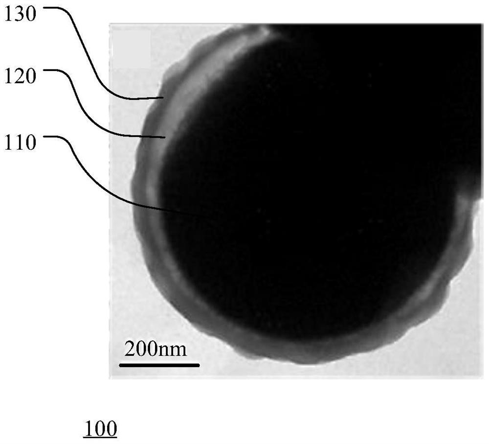
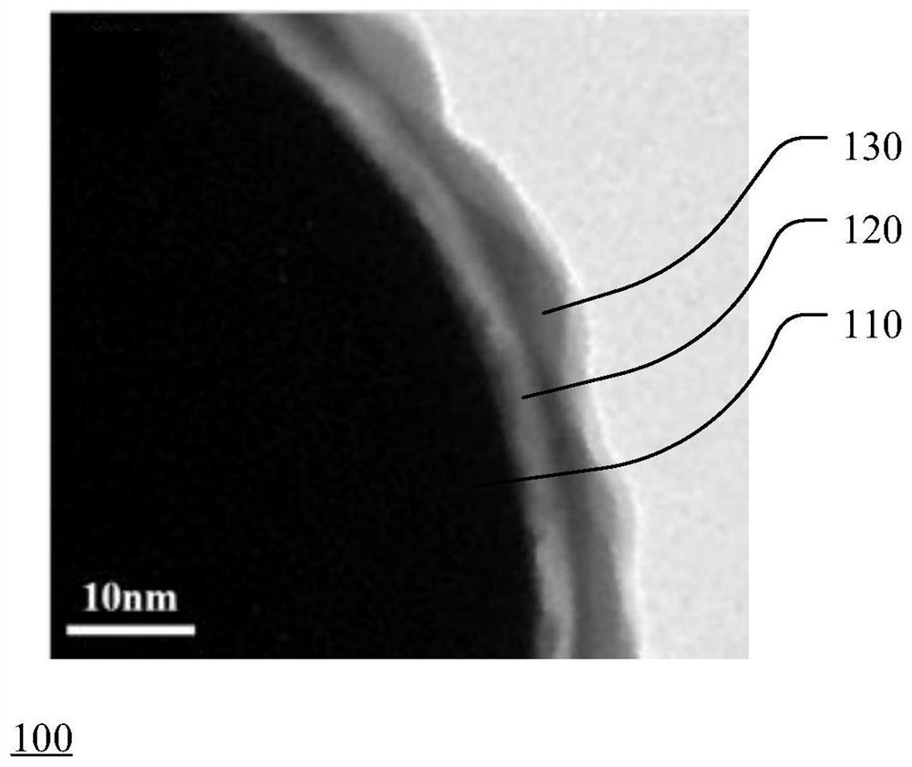
[0065] In step S23, the first precursor is trimethylsilane, and in step S25, the second precursor is O 2 , in step S27, the number of cycles is 100 times; in step S33, the third precursor is magnesium dicene, and in step S35, the fourth precursor is O 2 , in step S37, the number of loops is 3000 times. Therefore, in the absorbing material 110 of this embodiment, the core 110 is carbonyl iron powder particles; the sacrificial layer 121 is a silicon dioxide layer with a thickness of 5 nm; the insulating layer 130 is magnesium oxide with a thickness of 150 nm.
Embodiment 2
[0067] In step S23, the first precursor is trimethylsilane, and in step S25, the second precursor is O 2 , in step S27, the number of cycles is 100 times; in step S33, the third precursor is bis(ethylcyclopentadienyl) magnesium, in step S35, the fourth precursor is water, in step S37 , the number of cycles is 3000 times. Therefore, in the absorbing material 110 of this embodiment, the core 110 is carbonyl iron powder particles; the sacrificial layer 121 is a silicon dioxide layer with a thickness of 5 nm; the insulating layer 130 is magnesium oxide with a thickness of 150 nm.
PUM
| Property | Measurement | Unit |
|---|---|---|
| thickness | aaaaa | aaaaa |
| thickness | aaaaa | aaaaa |
| thickness | aaaaa | aaaaa |
Abstract
Description
Claims
Application Information


