

Multi-die fpga designed based on signal delay balance technology
A technology of signal delay and technical design, applied to semiconductor/solid-state device parts, semiconductor devices, electrical components, etc. Circuit requirements and other issues to achieve the effect of speeding up the design, reducing the difficulty of processing, and accelerating the convergence of design timing
- Summary
- Abstract
- Description
- Claims
- Application Information
AI Technical Summary
Problems solved by technology
Method used
Image

Examples
Embodiment Construction
[0044] The specific embodiments of the present invention will be further described below in conjunction with the accompanying drawings.
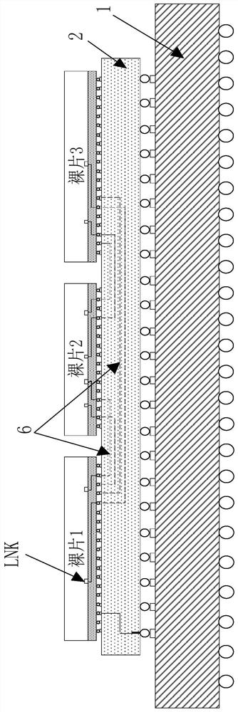
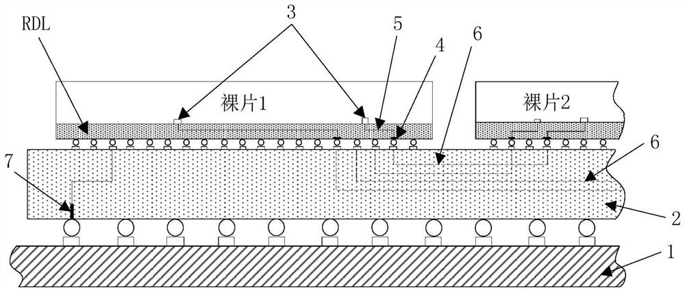
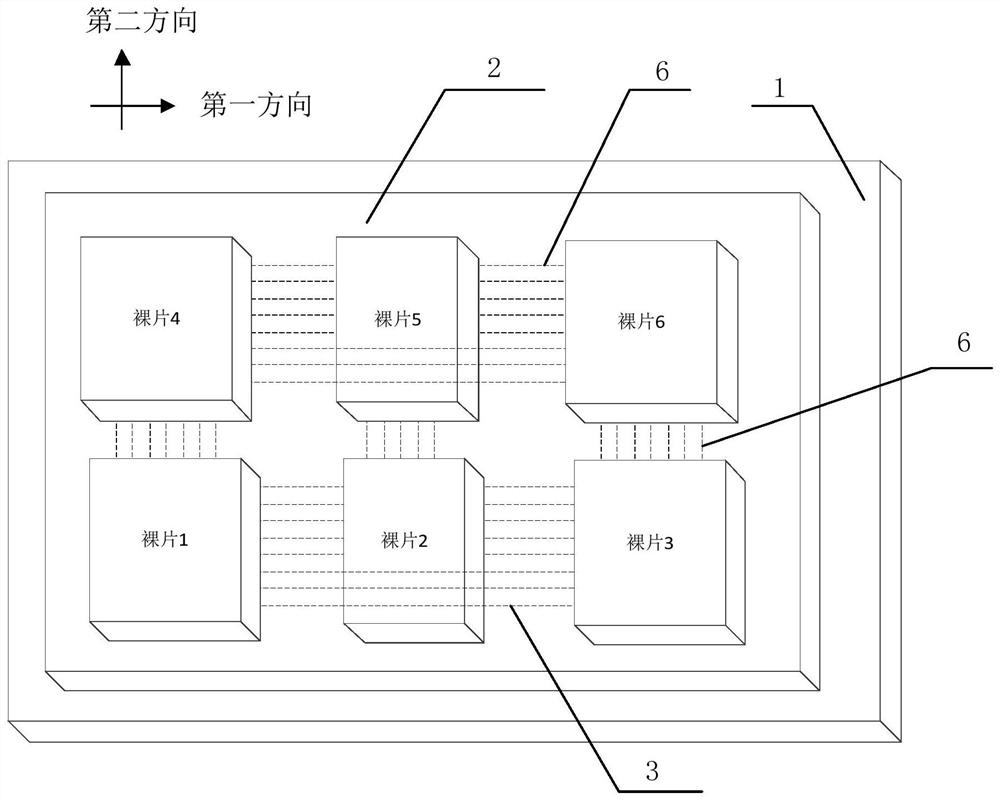
[0045] This application provides a multi-die FPGA based on signal delay balance technology design, figure 1 It is a schematic cross-sectional view of the packaging structure of the FPGA of the present application, figure 2 yes figure 1 Enlarged view of part of the structure, image 3 yes figure 1 The corresponding top view diagram. The FPGA includes a substrate 1, a silicon connection layer 2, and several FPGA dies that are stacked sequentially from bottom to top, such as in Figure 1-3 The structure shown contains 6 FPGA dice, denoted as dice 1-6 respectively. In actual implementation, the FPGA also includes a packaging shell packaged outside the substrate 1, the silicon connection layer 2 and the FPGA die to protect each component, and also includes pins for signal extraction connected to the substrate, etc. figure 1 and 2 These co...
PUM
 Abstract
Description
Claims
Application Information