Infrared thermopile sensing device

A technology of a thermopile sensor and a sensing device, applied in the field of infrared detectors, can solve the problems of inability to integrate a single-chip sensor and a processing circuit, low infrared absorption rate, disadvantageous low cost, and the like

Pending Publication Date: 2020-10-20
MEMSIC SEMICON WUXI
View PDF0 Cites 0 Cited by
  • Summary
  • Abstract
  • Description
  • Claims
  • Application Information

AI Technical Summary

Problems solved by technology

[0002] Most of the existing MEMS (Micro-Electro-Mechanical System, Micro-Electro-Mechanical System) thermopile structures are based on dedicated MEMS technology, which cannot integrate sensors and processing circuits on a single chip, which is not conducive to the development direction of low cost and high integration
In addition, the ther

Method used


Image

  • Infrared thermopile sensing device
  • Infrared thermopile sensing device
  • Infrared thermopile sensing device

Examples


Embodiment Construction

[0015] In order to make the above objects, features and advantages of the present invention more comprehensible, the present invention will be further described in detail below in conjunction with the accompanying drawings and specific embodiments.

[0016] Reference herein to "one embodiment" or "an embodiment" refers to a particular feature, structure or characteristic that can be included in at least one implementation of the present invention. "In one embodiment" appearing in different places in this specification does not all refer to the same embodiment, nor is it a separate or selective embodiment that is mutually exclusive with other embodiments. Unless otherwise specified, the words connected, connected, and joined in this document mean that they are electrically connected directly or indirectly.

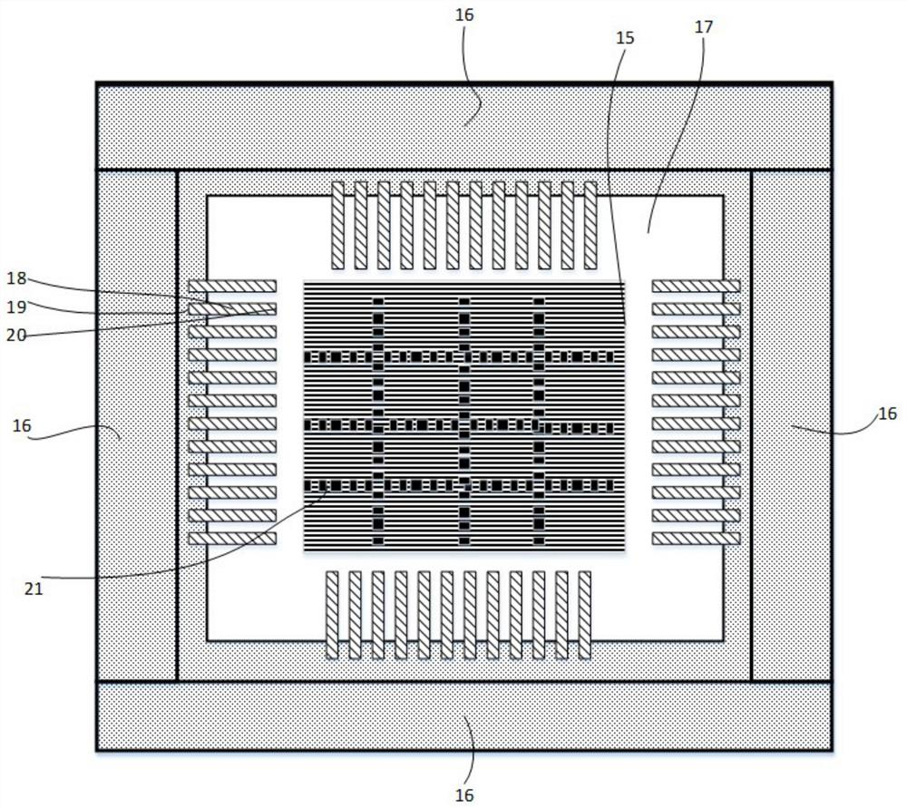
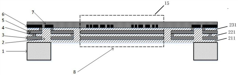
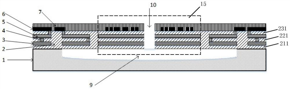
[0017] Please refer to figure 1 Shown, it is the top view of the infrared thermopile sensing device based on CMOS technology in one embodiment of the present invention; Pl...


PUM


Abstract

The invention provides an infrared thermopile sensing device. The device comprises a thermopile sensor formed on the basis of a substrate layer; the thermopile sensor comprises an absorption region; acavity is formed in the substrate layer; the absorption region is suspended above the cavity of the substrate layer; the absorption region comprises a first metal layer, a dielectric layer and a second metal layer which are stacked; the first metal layer is closer to the cavity of the substrate layer than the second metal layer; the dielectric layer of the absorption region is located between thefirst metal layer and the second metal layer; and the second metal layer of the absorption region is patterned to form a predetermined pattern. Thus, the infrared absorptivity is enhanced and the specific wavelength absorptivity is adjusted by making the metal layer into the predetermined pattern, so that the performance of the infrared thermopile sensing device is improved.

Description

【Technical field】 [0001] The invention belongs to the technical field of infrared detectors, in particular to an infrared thermopile sensing device based on CMOS technology. 【Background technique】 [0002] Most of the existing MEMS (Micro-Electro-Mechanical System, Micro-Electro-Mechanical System) thermopile structures are based on dedicated MEMS technology, which cannot integrate sensors and processing circuits on a single chip, which is not conducive to the development direction of low cost and high integration. In addition, the thermopile is produced on the standard CMOS (Complementary Metal Oxide Semiconductor) process. Due to the limitation of the CMOS standard process, the thickness of the film layer and the adjustable window of the material are narrow, resulting in low infrared absorption rate. The central absorption wavelength and application The requirements do not match. [0003] Therefore, it is necessary to propose a technical solution to overcome the above prob...

Claims


Application Information

Patent Timeline
IPC IPC(8): G01J5/12G01J5/16G01J5/10G01J5/00
CPCG01J5/12G01J5/16G01J5/10G01J5/0025G01J5/00G01J2005/123G01J2005/106G01J2005/103G01J5/485
Inventor 刘尧凌方舟蒋乐跃储莉玲
Owner MEMSIC SEMICON WUXI
Why Eureka
Try Eureka