Supercharge Your Innovation With Domain-Expert AI Agents!

OLED display panel bright spot defect correction system

A technology for display panel and bright spot defects, used in microscopes, instruments, electrical components, etc., can solve problems such as strict beam focusing requirements, poor repair system adaptability, and poor repair results, and achieve improved detail resolution, simple structure, The effect of uniform brightness

Pending Publication Date: 2020-10-27
BEIJING C&W ELECTRONICS GRP
View PDF0 Cites 1 Cited by
  • Summary
  • Abstract
  • Description
  • Claims
  • Application Information

AI Technical Summary

Problems solved by technology

In the field of OLED semiconductor display panel manufacturing, the existing technology uses a Gaussian laser beam to directly focus the way to repair the bright spot defects of the OLED display panel. Since the laser focal depth of the Gaussian beam under the repair parameters is generally less than 10 μm, the accuracy of laser focusing and It has high requirements for real-time performance and must be used in conjunction with the auto-focus system, which leads to strict requirements on the focus of the beam, poor adaptability of the entire repair system, and poor repair results

Method used


Image

  • OLED display panel bright spot defect correction system
  • OLED display panel bright spot defect correction system
  • OLED display panel bright spot defect correction system

Examples


Embodiment Construction

[0036] The principles and features of the present invention are described below in conjunction with the accompanying drawings, and the examples given are only used to explain the present invention, and are not intended to limit the scope of the present invention.

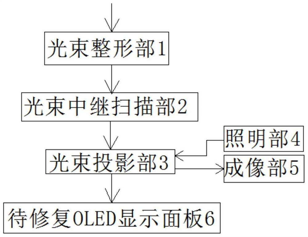
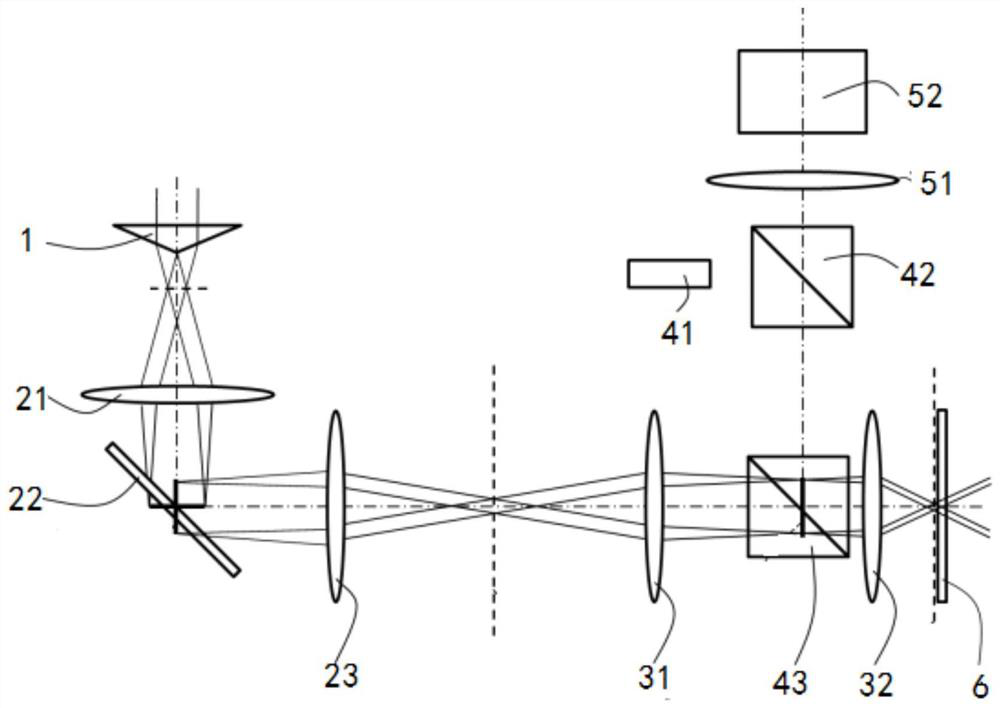
[0037] like figure 1 and Figure 5 As shown, this embodiment provides a bright spot defect correction system for an OLED display panel, including a beam shaping unit 1, a beam relay scanning unit 2, a beam projection unit 3, an illumination unit 4 and an imaging unit 5;

[0038] The beam shaping unit 1 is used to shape the incident Gaussian beam into a Gaussian-Bessel beam and output it, and the output optical path has a first Bessel region;

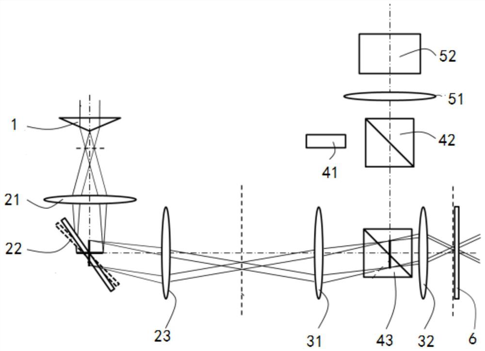
[0039] The beam relay scanning part 2 is arranged on the output optical path of the beam shaping part 1, which is used to relay the Gauss-Bessel beam output by the beam shaping part 1 to the far field, and make the Gaussian - Bessel beam off-axis and beam scanning;

[0040]...


PUM

PropertyMeasurementUnit
diameteraaaaaaaaaa

Abstract

The invention discloses a bright spot defect correction system for an OLED display panel. The bright spot defect correction system comprises a light beam shaping part, a light beam relay scanning part, a light beam projection part, an illumination part and an imaging part, wherein the light beam shaping part is used for shaping an incident Gaussian light beam into a Gaussian-Bessel light beam andoutputting the Gaussian-Bessel light beam, the light beam relay scanning part is arranged on an output light path of the light beam shaping part, the light beam projection part is arranged on an output light path of the light beam relay scanning part, a to-be-repaired OLED display panel is arranged at a light beam focusing position behind the light beam projection part, a light beam focusing pointbehind the light beam projection part is aligned to a bright spot defect area of the to-be-repaired OLED display panel, the illumination part is arranged on a light path in the light beam projectionpart, and the imaging part is arranged on a retroreflection light path of the illumination part. The system is more convenient to operate and higher in repair efficiency.

Description

technical field [0001] The invention belongs to the field of laser equipment, and in particular relates to a system for correcting bright spot defects of an OLED display panel. Background technique [0002] In the field of semiconductor display, semiconductor display panel automatic repair equipment based on laser technology has increasingly become one of the indispensable and important equipment. Its main requirements include the process improvement of the original production line, and the repair "beautiful" of waste display defect products And the supporting construction of new high-generation production lines. In the field of OLED semiconductor display panel manufacturing, the existing technology uses a Gaussian laser beam to directly focus the way to repair the bright spot defects of the OLED display panel. Since the laser focal depth of the Gaussian beam under the repair parameters is generally less than 10 μm, the accuracy of laser focusing and It has high requirement...

Claims


Application Information

Patent Timeline
Patent Type & Authority Applications(China)
IPC IPC(8): G02B21/06G02B26/10G02B27/09H01L51/56
CPCG02B27/0927G02B27/0955G02B26/10G02B21/06H10K71/861H10K71/00
Inventor 刘欣王馨莹李剑平王福旺孟鹏飞张亚辉李立锋林涛
Owner BEIJING C&W ELECTRONICS GRP
Features
  • R&D
  • Intellectual Property
  • Life Sciences
  • Materials
  • Tech Scout
  • Unparalleled Data Quality
  • Higher Quality Content
  • 60% Fewer Hallucinations
Learn More