Capacitor and forming method thereof, DRAM unit and memory
A technology of capacitors and capacitors, which is applied in the direction of capacitors, electrical components, electric solid devices, etc., and can solve problems such as prone to collapse
- Summary
- Abstract
- Description
- Claims
- Application Information
AI Technical Summary
Problems solved by technology
Method used
Image
Examples
Embodiment Construction
[0027] As mentioned in the background art, the integration level of capacitors in the prior art needs to be further improved.
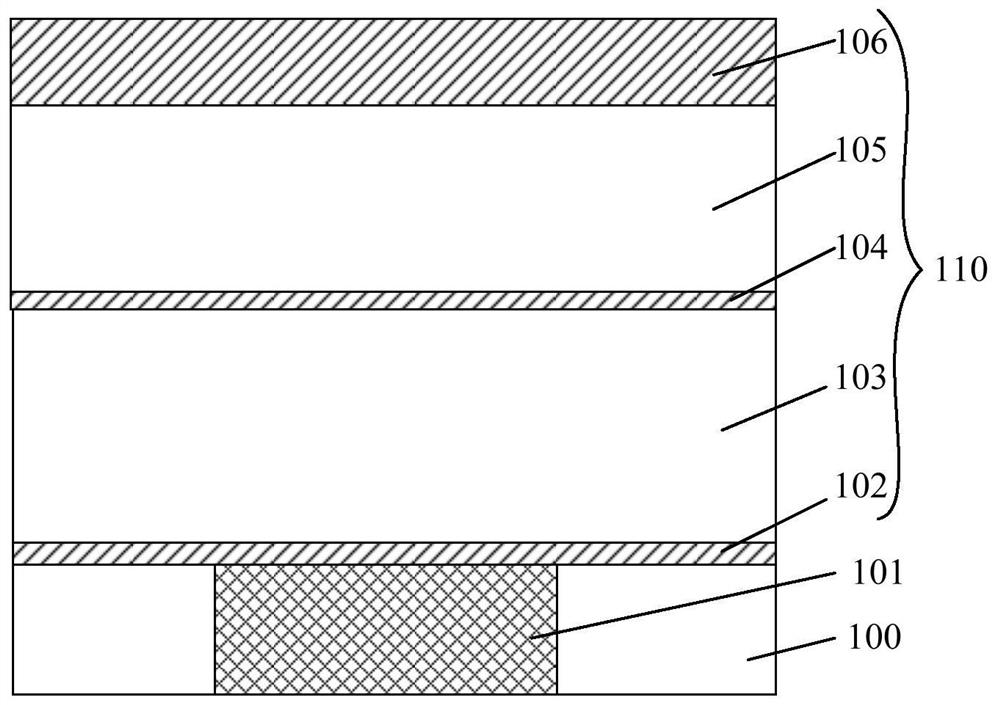
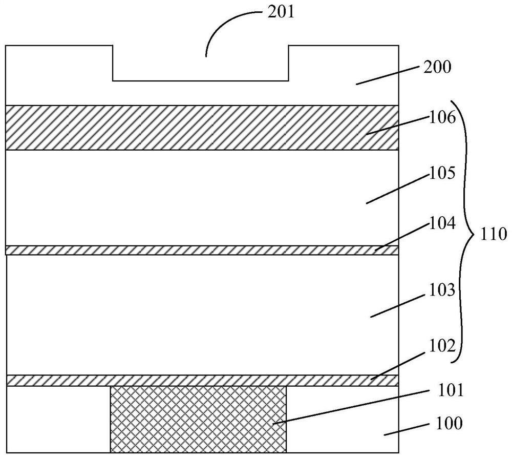
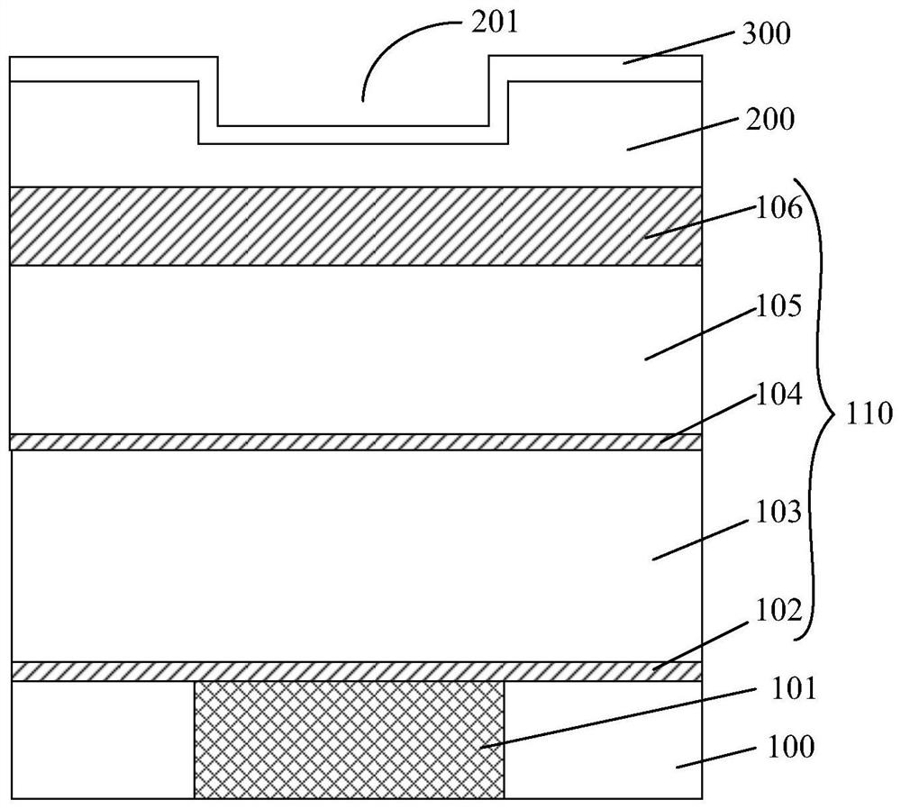
[0028] In order to solve the above problems, the applicant proposes a new capacitor and its forming method. In order to further improve the integration of the capacitor, more than two U-shaped lower electrode layers may be formed in one capacitor and connected to the same electrical contact portion. To form more than two U-shaped lower electrode layers, it is necessary to form more than two capacitance holes on one electrical contact portion, and the critical size of the capacitance holes is greatly reduced. Under the current process conditions, it is difficult to realize through the existing photolithography and etching process. Even if the capacitor hole with smaller size can be formed through the double patterning process, multiple photolithography and etching are required, and the process cost is greatly increased. . Applicants have overcome the...
PUM
 Abstract
Description
Claims
Application Information


