Semiconductor device and method of forming the same

A semiconductor and device technology, applied in the field of semiconductor devices and their formation, can solve the problems of miniaturization and miniaturization of semiconductor devices, and small unit capacitance value of capacitors, so as to improve the capacitance value per unit area, reduce process costs, and optimize electrical performance. Effect

Active Publication Date: 2017-11-03
SEMICON MFG INT (SHANGHAI) CORP
View PDF6 Cites 0 Cited by
  • Summary
  • Abstract
  • Description
  • Claims
  • Application Information

AI Technical Summary

Problems solved by technology

[0005] However, in the existing semiconductor device technology, the unit capacitance value of the formed capacitor is small. In order to increase the capacitance of the semiconductor device, the area of ​​the semiconductor device has to be increased, which is not conducive to the development of semiconductor devices in the direction of miniaturization and miniaturization.

Method used


Image

  • Semiconductor device and method of forming the same
  • Semiconductor device and method of forming the same
  • Semiconductor device and method of forming the same

Examples


Embodiment Construction

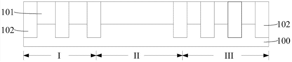
[0034] It can be seen from the background art that the capacitance of semiconductor devices formed in the prior art is small, and it is difficult to meet the demand for capacitance of semiconductor devices, resulting in an increase in chip area, which is not conducive to meeting the development trend of device miniaturization.

[0035] In order to solve the above problems, the manufacturing method of semiconductor devices in the prior art is studied. In order to save chip area and improve production efficiency, active regions, tunneling dielectric layers, floating gate polysilicon layers, ONO (oxide-nitride-oxide) dielectrics are used layer and the control gate polysilicon layer constitute a capacitor of the semiconductor device, the capacitor including a first capacitor and a second capacitor.

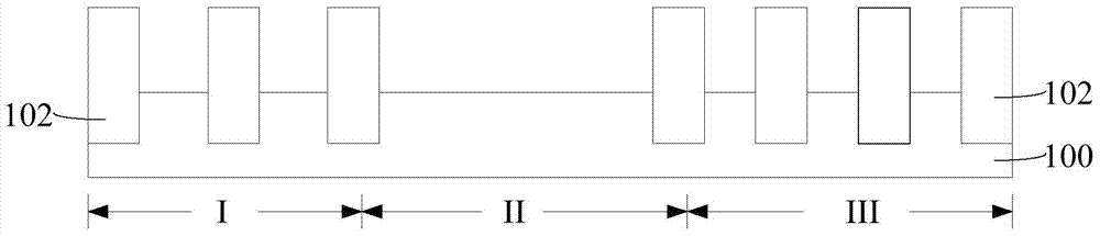
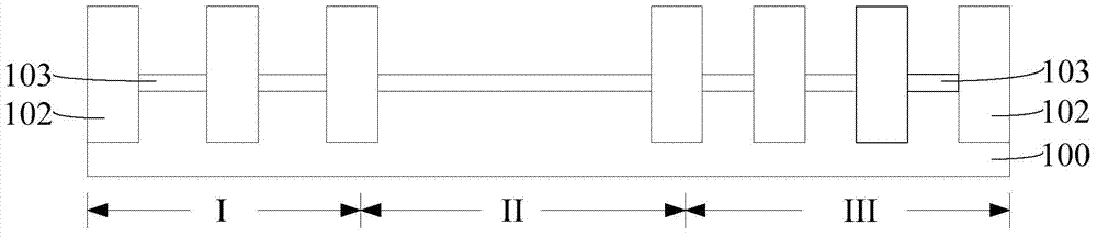
[0036] Define the active region as the lower electrode layer, the tunnel dielectric layer as the lower insulating layer, the floating gate polysilicon layer as the middle electrode lay...


PUM


Abstract

A semiconductor device and a method for forming the same, wherein the method for forming the semiconductor device includes: providing a substrate, the substrate includes a first region, a second region, and a third region, and an initial isolation layer is formed in the substrate; sequentially forming a tunnel dielectric layer and a floating gate conductive layer on the surface of the substrate between the initial isolation layers; forming an inter-gate dielectric layer covering the surface of the floating gate conductive layer; while removing the inter-gate dielectric layer in the first region, removing The inter-gate dielectric layer in the second region; while the gate oxide layer is formed on the surface of the substrate in the first region, a gate oxide layer is formed on the surface of the floating gate conductive layer in the second region, and the thickness of the gate oxide layer is smaller than the thickness of the inter-gate dielectric layer ; forming a control gate conductive layer covering the gate dielectric layer in the first region and the second region, and the surface of the inter-gate dielectric layer in the third region. The invention increases the capacitance value per unit area of ​​the semiconductor device, optimizes the electrical performance of the semiconductor device, and meets the development trend of miniaturization and miniaturization of the semiconductor device.

Description

technical field [0001] The invention relates to the technology in the field of semiconductor manufacturing, in particular to a semiconductor device and a forming method thereof. Background technique [0002] In the current semiconductor industry, integrated circuit products can be mainly divided into three types: logic, memory and analog circuits, among which memory devices account for a considerable proportion of integrated circuit products. Among storage devices, the development of flash memory (flash memory for short) is particularly rapid in recent years. Its main feature is that it can keep stored information for a long time without power on, and has many advantages such as high integration, fast access speed, easy erasure and rewriting, etc. The field has been widely used. [0003] With the development of semiconductor technology, storage devices are more widely used, and the storage device and other device regions need to be formed on a chip at the same time to form...

Claims


Application Information

Patent Timeline
Patent Type & Authority Patents(China)
IPC IPC(8): H01L27/06H01L21/784
Inventor 宁先捷
Owner SEMICON MFG INT (SHANGHAI) CORP
Why Eureka
Try Eureka