Capacitance dielectric layer and its forming method and capacitor

A dielectric layer and capacitor technology, applied in the direction of electric solid devices, circuits, electrical components, etc., can solve the problems of increasing leakage current, data loss, affecting process reliability and yield, etc., to improve the capacitance value per unit area, reduce The effect of thickness

Inactive Publication Date: 2007-09-12
UNITED MICROELECTRONICS CORP
View PDF0 Cites 14 Cited by
  • Summary
  • Abstract
  • Description
  • Claims
  • Application Information

AI Technical Summary

Problems solved by technology

At present, the capacitor dielectric layer is generally formed by a single deposition method. If the thickness of the capacitor dielectric layer is directly reduced in the same way, the formed capacitor dielectric layer, especially the part of the silicon nitride layer , it is easy to produce defects 130 such as tiny cracks (seam) or pinholes (pinhole), and these defects will become the leakage current path, which will increase the leakage current and reduce the breakdown voltage, and even cause data loss, thereby affecting Process reliability and yield

Method used


Image

  • Capacitance dielectric layer and its forming method and capacitor
  • Capacitance dielectric layer and its forming method and capacitor
  • Capacitance dielectric layer and its forming method and capacitor

Examples


Embodiment Construction

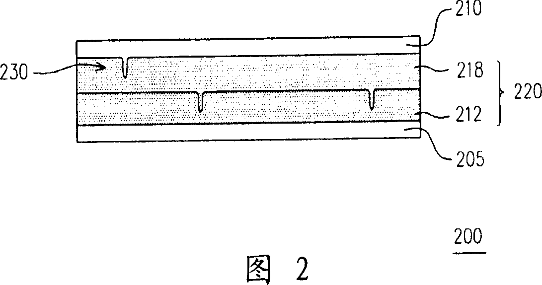
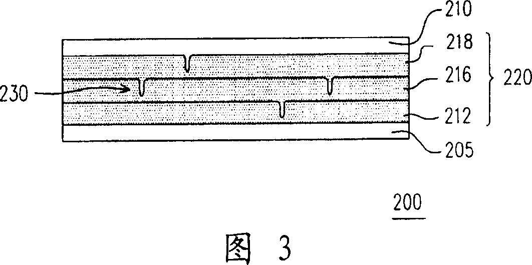
[0049] FIG. 2 is a schematic cross-sectional view of a capacitor dielectric layer according to an embodiment of the present invention.

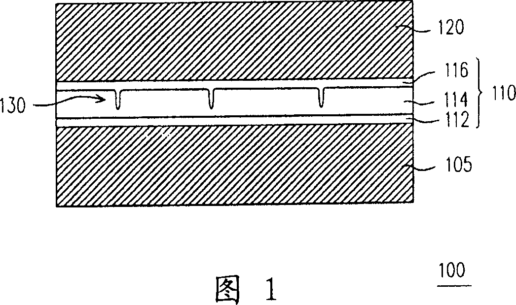
[0050] Referring to FIG. 2 , the capacitor dielectric layer 200 of the present invention includes a dielectric layer 205 , a dielectric layer 210 and a silicon nitride stack 220 . Wherein, the material of the dielectric layer 205 can be selected from one of silicon oxide, silicon nitride, silicon carbide, silicon oxynitride, silicon carbide nitride or silicon oxycarbide, and the material of the dielectric layer 210 can be selected from One of silicon oxide, silicon nitride, silicon carbide, silicon oxynitride, silicon carbide nitride, or silicon oxycarbide. Of course, the dielectric layer 205 and the dielectric layer 210 can also be other dielectric materials, for example. The thickness of the dielectric layer 205 is, for example, between 90 angstroms and 110 angstroms, the thickness of the dielectric layer 210 is, for example, between 90 an...


PUM

PropertyMeasurementUnit
thicknessaaaaaaaaaa
thicknessaaaaaaaaaa

Abstract

The invention is a capacitor's dielectric layer, comprising first dielectric layer, second dielectric layer and silicon nitride stack, where the silicon nitride stack is located between the first and second dielectric layers; and by reducing thickness, it can raise unit area capacitance value and can avoid causing the problems of leakage current increase and breakdown voltage decrease.

Description

technical field [0001] The invention relates to a semiconductor element and a forming method thereof, in particular to a capacitor dielectric layer, a forming method thereof and a capacitor. Background technique [0002] In recent years, with the rapid development of the integrated circuit industry, the miniaturization and integration of components have also been continuously improved. Therefore, the design of the entire circuit component size needs to advance in the direction of continuous reduction in size. [0003] Please refer to FIG. 1 , which is a schematic cross-sectional view of a conventional capacitor. Generally speaking, the capacitor 100 is mainly composed of the lower electrode plate 105 , the capacitor dielectric layer 110 and the upper electrode plate 120 . Wherein, the material of the upper electrode plate 120 is polysilicon, and the material of the lower electrode plate 105 is polysilicon. The capacitor dielectric layer 110 is composed of a triple structur...

Claims


Application Information

Patent Timeline
Patent Type & Authority Applications(China)
IPC IPC(8): H01L27/00H01L27/02H01L27/06H01L27/102H01L27/108H01L29/92H01L21/00H01L21/02H01L21/31H01L21/82H01L21/8222H01L21/8242H10B12/00
Inventor 王之俊陈新兴蒋裕和
Owner UNITED MICROELECTRONICS CORP
Why Eureka
Try Eureka