A display panel and its manufacturing method
A display panel and display area technology, which is applied in the fields of final product manufacturing, sustainable manufacturing/processing, semiconductor/solid-state device manufacturing, etc., can solve problems such as reducing the screen ratio of display panels, and achieve the effect of reducing manufacturing costs
- Summary
- Abstract
- Description
- Claims
- Application Information
AI Technical Summary
Problems solved by technology
Method used
Image

Examples
Embodiment 1
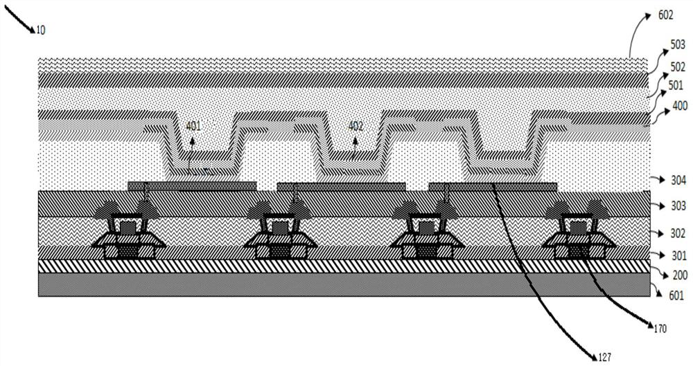
[0038] Such as figure 1 As shown, in this embodiment, the display panel 10 of the present invention includes a substrate 601, a light emitting layer 120, a barrier layer 200, a first insulating layer 301, a second insulating layer 302, a flat layer 303, a thin film transistor unit 170, and a conductive unit 127 The pixel definition layer 304 and the cathode layer 407 .
[0039] The substrate 601 is a flexible substrate or a rigid substrate, which is used for receiving other film layers of the display panel 10 and also plays a protective role.
[0040] The barrier layer 200 is disposed on one side of the substrate 601. Since the barrier layer 200 is usually used to prepare various electrical components and is sensitive to external water vapor impurities, the barrier layer 200 can isolate external water vapor impurities and improve the service life of the electrical components.
[0041] The TFT unit 170 includes an active layer, a gate layer, a source layer and a drain layer. ...
PUM
 Abstract
Description
Claims
Application Information
 - R&D
- Intellectual Property
- Life Sciences
- Materials
- Tech Scout
- Unparalleled Data Quality
- Higher Quality Content
- 60% Fewer Hallucinations
Browse by: Latest US Patents, China's latest patents, Technical Efficacy Thesaurus, Application Domain, Technology Topic, Popular Technical Reports.
© 2025 PatSnap. All rights reserved.Legal|Privacy policy|Modern Slavery Act Transparency Statement|Sitemap|About US| Contact US: help@patsnap.com