Semiconductor device and producing method thereof

A semiconductor and device technology, applied in the field of semiconductor devices and their manufacturing, can solve problems such as large resistance value, poor high-frequency characteristics, and no practical and effective manufacturing methods

Inactive Publication Date: 2003-08-20
NEC CORP
View PDF0 Cites 0 Cited by
  • Summary
  • Abstract
  • Description
  • Claims
  • Application Information

AI Technical Summary

Problems solved by technology

[0009] However, the application of this structure to Bi-CMOS is not described at all in these prior art
Therefore, there is still no practical and efficient fabrication method
In addition, since the resistance value of the polysilicon portion becomes large, this structure causes a problem of poor high-frequency characteristics

Method used


Image

  • Semiconductor device and producing method thereof
  • Semiconductor device and producing method thereof
  • Semiconductor device and producing method thereof

Examples


no. 1 example

[0085] Referring to the accompanying drawings, the first manufacturing method of the present invention will be described in detail below.

[0086] First, refer to image 3 . On the silicon substrate 30, in the region intended to be the formation region 33 of the bipolar transistor, an n as a collector electrode is formed. + Buried layer 2, p + Buried layer 3. Next, an epitaxial layer 4 having a thickness of about 1 to 2 μm and a resistance of 0.5 to 2 Ω·cm is grown on the surface. Then a local oxidation of silicon (LOCOS) oxide film 1 (field oxide film) is formed with a thickness of 200-400 nm to isolate elements from each other. At this time, a LOCOS oxide film is formed to cover the entire surface of the capacitor formation region 32 . Next, an n well is formed in the p-MOS formation region 34, and next, a p well 5 is formed in the n-MOS formation region 34, thereby completing image 3 manufacturing steps.

[0087] Pass 1~5×10 13 cm -2 Phosphorus implanted with an a...

no. 2 example

[0099] Referring to the accompanying drawings, the second manufacturing method of the present invention will be described in detail.

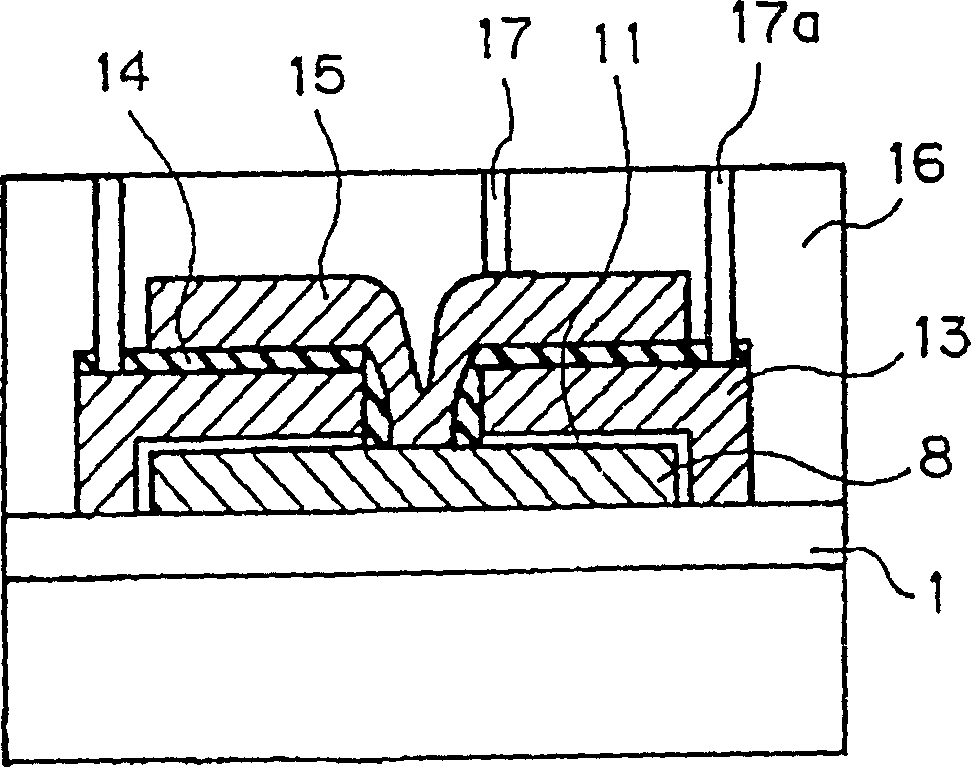
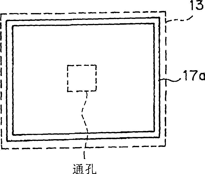
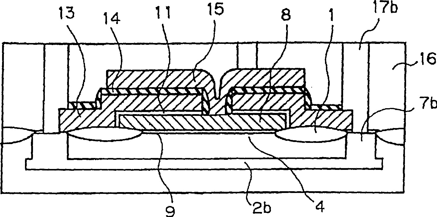
[0100] First, as in the first embodiment, n + buried layers 2 and p + Buried layer 3. After growing epitaxial layer 4 on the surface, LOCOS oxide film 1 (field oxide film) is formed, after which n well 6 and p well 5 are formed by ion implantation. Also, in this example, n + The buried layer 2b is provided under the capacitor forming region 32 as Figure 11 shown. the n + The buried layer 2b functions as the fourth electrode of the capacitor. Considering the LOCOS oxide film 1 in the capacitor formation region 32, it can be set as Figure 11 In the label 1b, set aside the central part as a window. Or in the capacitor forming region, the LOCOS oxide film represented by numeral 1b is not formed at all.

[0101] Next, to form n + The contact of the buried layer 2 is formed under similar conditions to the first embodiment n + Collector g...


PUM


Abstract

A semiconductor device having a capacitor, a bipolar transistor and complementary MOSFETs on a semiconductor substrate, the capacitor being constituted from a first electrode, a second electrode 13 separated from the first electrode by an insulating film 11 and a third electrode 15 separated from the second electrode by another insulating film 14 and connected to the first electrode is manufactured; where all electrodes in the capacitor and insulating films between them are formed simultaneously with other manufacturing steps of a bipolar transistor or the MOSFETs. This manufacturing method can produce a semiconductor device such as a Bi-CMOS and the like, which is capable of large scale integration and has a capacitor with a large capacitance but occupying only a small area.

Description

technical field [0001] The present invention relates to semiconductor devices having capacitors, bipolar transistors and complementary metal-oxide-semiconductor field-effect transistors (MOSFETs) and methods of manufacturing the same. Background technique [0002] Recently, there is a need to increase a larger capacitance value for Bi-CMOS LSI in which complementary metal-oxide-semiconductor (CMOS) with large-scale integration and low power consumption and bipolar transistors with fast performance are formed on the same on the semiconductor substrate. [0003] In Japanese Patent Application Laid-Open No. 22054 / 1989, there is disclosed a method of fabricating a capacitor in a semiconductor device in which a MOSFET and a bipolar transistor are located on the same substrate. In this method, one electrode of the capacitor is formed at the same time as the gate electrode of the MOSFET, and after the insulating film of the capacitor is formed, the other electrode of the capacitor...

Claims


Application Information

Patent Timeline
Patent Type & Authority Patents(China)
IPC IPC(8): H01L27/04H01L21/02H01L21/822H01L21/8249H01L27/06
CPCH01L27/0688H01L28/40H01L21/8249H01L29/78
Inventor 藤井宏基
Owner NEC CORP
Why Eureka
Try Eureka