Field-effect transistor

a field-effect transistor and transistor technology, applied in the field of field-effect transistors, can solve the problem of extremely difficult fabrication, and achieve the effect of low electric power consumption

Inactive Publication Date: 2012-03-01
HOKKAIDO UNIVERSITY +1
View PDF4 Cites 58 Cited by
  • Summary
  • Abstract
  • Description
  • Claims
  • Application Information

AI Technical Summary

Benefits of technology

[0046]The field-effect transistor of the present invention can realize a super low electric power consumption and super large scale integration that a conventional CMOS circuit has while enjoying super high-speed properties that a graphene material has.

Problems solved by technology

However, the above-described means each have the following problems.
For this reason, the channel width must be adjusted in an atomic order of several nanometers or less, and this is difficult by the current processing technique.
Also, in the case of bilayer graphene by outside electric field application, a double gate structure having a gate in the upper and lower parts is needed, and the fabrication is extremely difficult.

Method used


Image

  • Field-effect transistor
  • Field-effect transistor
  • Field-effect transistor

Examples


Embodiment Construction

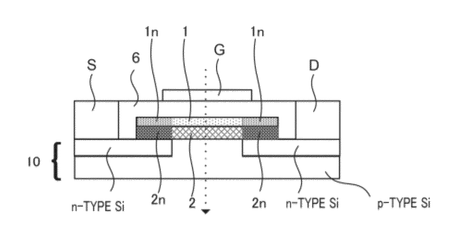
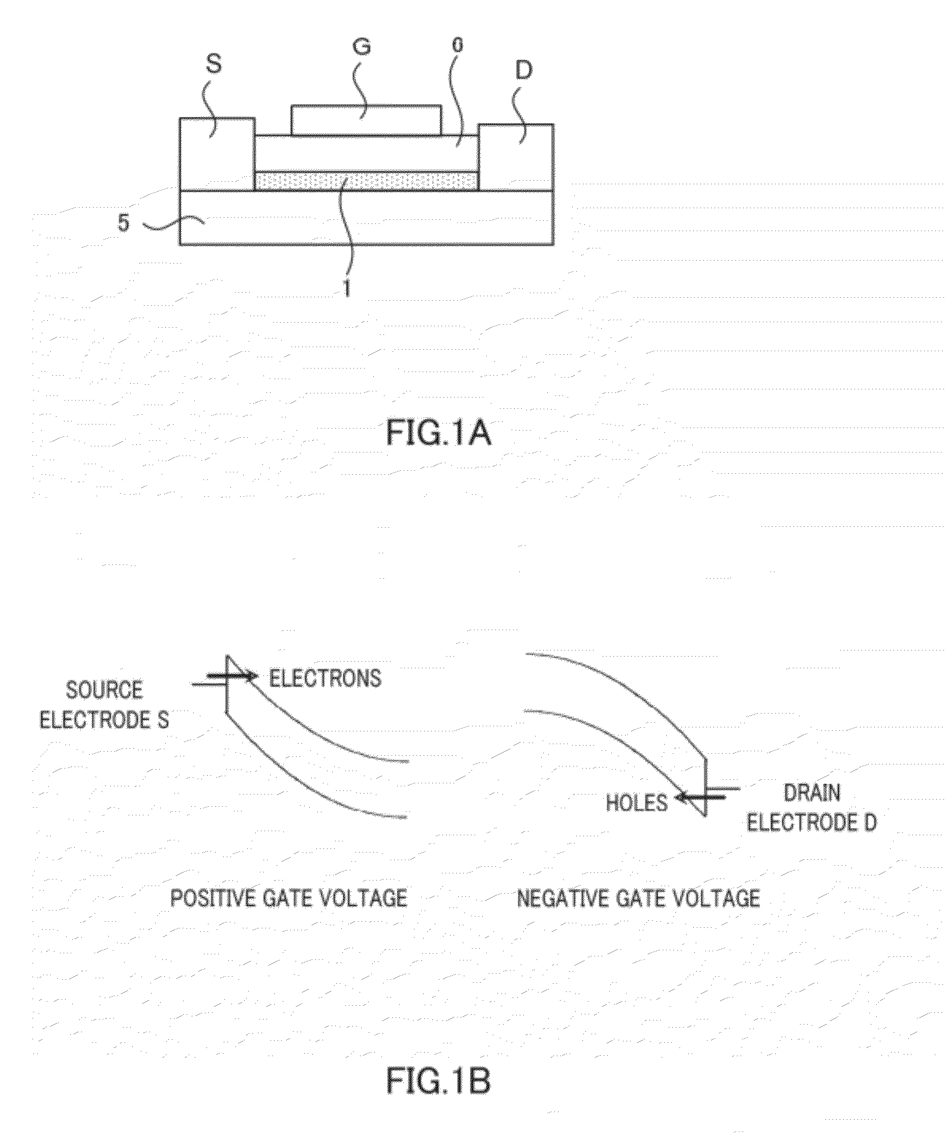
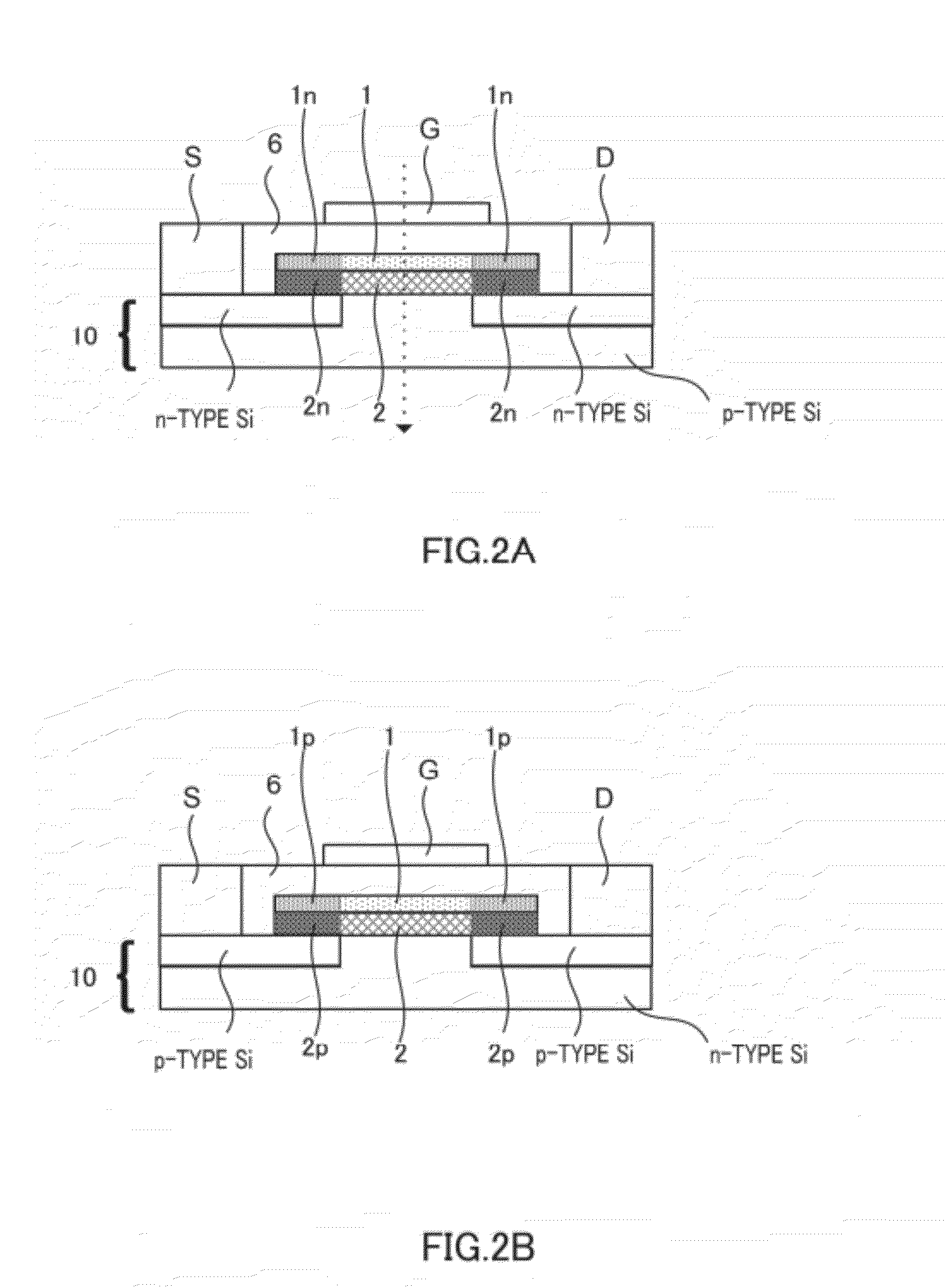
[0056]A field-effect transistor of the present invention has a semiconductor substrate, a channel including a graphene layer, source and drain electrodes, and a gate electrode. The field-effect transistor of the present invention may be an n-type field-effect transistor or may be a p-type field-effect transistor. The channel including a graphene layer and the source and drain electrodes are not in direct contact but are connected via a semiconductor layer.

[0057]The semiconductor substrate of the field-effect transistor of the present invention is not particularly limited, but is preferably a silicon substrate. This is because, as described later, a graphene layer that will be a channel must be disposed on the semiconductor substrate; and a silicon carbide layer that will be a precursor of the graphene layer can be epitaxially grown on a silicon substrate.

[0058]Further, the semiconductor substrate in the n-type field-effect transistor may be a p-type silicon substrate; and the semico...


PUM


Abstract

The disclosed field-effect transistor has a graphene channel, and does not exhibit ambipolar properties. Specifically, the field-effect transistor has a semi-conducting substrate; a channel including a graphene layer disposed on the aforementioned semiconductor substrate; a source electrode and drain electrode comprising a metal; and a gate electrode. The aforementioned channel and the aforementioned source and drain electrodes comprising a metal are connected via a semiconductor layer.

Description

TECHNICAL FIELD[0001]The present invention relates to a field-effect transistor, and more specifically to a field-effect transistor having a graphene channel.BACKGROUND ART[0002]The field-effect transistor has a channel made of a semiconductor, a source electrode and a drain electrode that are in contact with the channel, and a gate electrode that controls the electric current flowing through the channel. Further, a field-effect transistor in which the channel is made of graphene is also proposed (See, for example, Patent Literature 1).[0003]Graphene is generally a monolayer sheet having a six-membered ring structure made of carbon atoms. Since graphene is outstandingly excellent in electron transportation properties as compared with any of the already existing semiconductors, a field-effect transistor having a channel made of graphene is expected to be capable of outstandingly improving the speed performance of a transistor that faces a miniaturization limit. However, ideal graphen...

Claims


Application Information

Patent Timeline
Patent Type & Authority Applications(United States)
IPC IPC(8): H01L29/08H01L29/12B82Y99/00
CPCH01L21/02527H01L21/02573H01L21/02612H01L21/8213H01L21/823807H01L29/78684H01L29/165H01L29/66431H01L29/7781H01L29/78618H01L29/1606
Inventor SANO, EIICHIOTSUJI, TAIICHI
Owner HOKKAIDO UNIVERSITY
Why Eureka
Try Eureka