Display panel and display device

A display panel and column technology, applied in the field of display panels and display devices, can solve the problems of reduced distance and unbalanced parasitic capacitance, and achieve the effects of avoiding noise, balancing the overall consistency, and improving the touch point reporting rate and sensitivity.

Pending Publication Date: 2020-11-06
WUHAN CHINA STAR OPTOELECTRONICS SEMICON DISPLAY TECH CO LTD
View PDF0 Cites 4 Cited by
  • Summary
  • Abstract
  • Description
  • Claims
  • Application Information

AI Technical Summary

Problems solved by technology

[0004] The present application provides a display panel and a display device, which solve the problem of unbalanced parasitic capacitance due to the smaller distance between the cathode layer at the column and the touch function layer

Method used


Image

  • Display panel and display device
  • Display panel and display device
  • Display panel and display device

Examples


Embodiment Construction

[0026] The technical solutions in the embodiments of the present application will be clearly and completely described below in conjunction with the drawings in the embodiments of the present application. Apparently, the described embodiments are only some of the embodiments of this application, not all of them. Based on the embodiments in this application, all other embodiments obtained by those skilled in the art without making creative efforts belong to the scope of protection of this application.

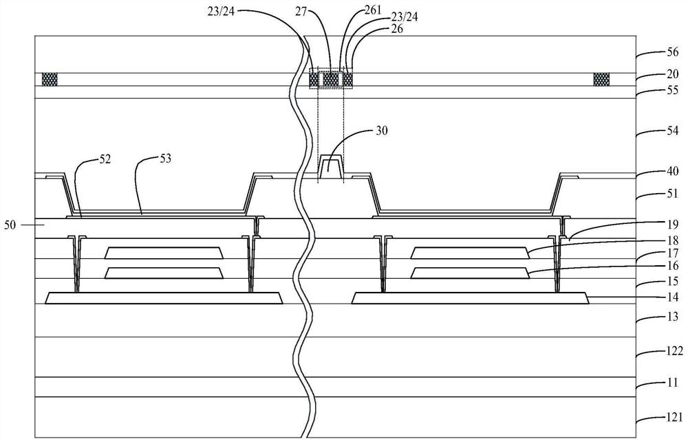
[0027] Such as figure 1 , figure 2 As shown, in one of the embodiments, the display panel or display device may include, but is not limited to, an anode layer 52 , a pixel definition layer 51 , a light emitting layer 53 , a cathode layer 40 and a touch function layer 20 that are sequentially stacked. Wherein, a column 30 is arranged between the pixel definition layer 51 and the cathode layer 40, and the column 30 raises the corresponding position of the cathode layer 40, so th...


PUM


Abstract

The invention discloses a display panel and a display device. A winding structure with a hollow part is arranged on an electrode wire of a touch function layer, and the parasitic capacitance between the touch function layer and the cathode layer at the stand column can be reduced, so that the overall consistency of the parasitic capacitance between the touch function layer and the cathode layer isbalanced, noise caused by unbalanced parasitic capacitance is avoided, and the overall touch reporting rate and sensitivity are improved.

Description

technical field [0001] The present application relates to the field of display technology, in particular to the field of touch technology, and in particular to a display panel and a display device. Background technique [0002] Flexible organic light-emitting diode (OLED, Organic Light-Emitting Diode) display has the advantages of active light emission, large viewing angle, wide color gamut, high brightness, fast response speed, low power consumption, and structural bendability, etc., and is increasingly popular in the market. There is a tendency to gradually replace LCD (Liquid Crystal Display, liquid crystal display) as the mainstream of display technology. [0003] In the conventional technical solution, a pixel define layer (PDL, pixel define layer) is disposed on one side of the substrate, and a post (PS, photo spacer) is disposed on the surface of the pixel define layer. During the OLED evaporation process, the column is used to support a high-precision metal mask (FM...

Claims


Application Information

Patent Timeline
Patent Type & Authority Applications(China)
IPC IPC(8): H01L27/32G09F9/30
CPCG09F9/301H10K59/40H10K59/179H10K59/122G06F3/0412G06F3/0446G06F2203/04112G06F2203/04111G06F3/0448H10K59/126G06F2203/04102
Inventor 叶剑
Owner WUHAN CHINA STAR OPTOELECTRONICS SEMICON DISPLAY TECH CO LTD
Why Eureka
Try Eureka