Array substrate, backlight module, display panel, display device and preparation method

An array substrate and column direction technology, which is applied in the fields of display devices and preparation, display panels, backlight modules, and array substrates, can solve the problems of complex array substrate preparation process and high production cost, and achieve saving of masks and preparation processes, The effect of simplifying the preparation process and reducing the manufacturing cost

Active Publication Date: 2020-11-10
SHANGHAI TIANMA MICRO ELECTRONICS CO LTD
View PDF3 Cites 4 Cited by
  • Summary
  • Abstract
  • Description
  • Claims
  • Application Information

AI Technical Summary

Problems solved by technology

Although the process of setting the light-shielding layer ensures the performance of the thin film transistor, it needs to set up two additional masks and add two manufacturing processes, which makes the manufacturing process of the array substrate more complicated and the production cost becomes higher.

Method used


Image

  • Array substrate, backlight module, display panel, display device and preparation method
  • Array substrate, backlight module, display panel, display device and preparation method
  • Array substrate, backlight module, display panel, display device and preparation method

Examples


Embodiment Construction

[0042] The present invention will be further described in detail below in conjunction with the accompanying drawings and embodiments. It should be understood that the specific embodiments described here are only used to explain the present invention, rather than to limit the present invention. In addition, it should be noted that, for the convenience of description, only some parts related to the present invention are shown in the drawings but not all structures.

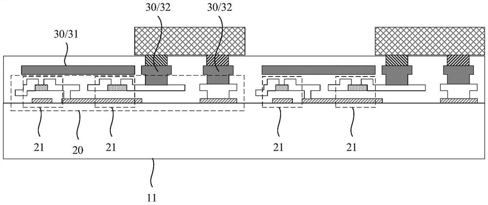
[0043] As mentioned in the background technology section, in the existing panel preparation process, in order to prevent the thin film transistor from being affected by light, it is generally necessary to set up a light-shielding layer for light-shielding. figure 1 is a schematic diagram of the structure of the existing array substrate, refer to figure 1, in the array substrate, the drive unit 20 provided on the base substrate 11 includes a thin film transistor 21, and the side of the thin film transistor 21 away f...


PUM


Abstract

The embodiment of the invention discloses an array substrate, a backlight module, a display panel, a display device and a preparation method. The array substrate comprises a plurality of driving units. Each driving unit comprises a first electrode, a second electrode and at least one thin film transistor; the first electrode and the second electrode are used for being connected with the anode andthe cathode of a light emitting diode respectively, so that the vertical projection of the light emitting diode on the array substrate can be overlapped with the at least one thin film transistor, andthe thin film transistor is located at the backlight side of the light emitting diode in the light emitting direction of the light emitting diode. The driving unit controls the light-emitting diode to be turned on or off according to the driving signal. According to the embodiment of the invention, the problem that an existing array substrate needs to be additionally provided with a shading layer, so that the preparation process is complex, is solved; the influence of external illumination on the thin film transistor can be avoided, masks and preparation procedures required for preparing theshading layer are saved, the preparation process of the array substrate is simplified, and the manufacturing cost is reduced.

Description

technical field [0001] The embodiments of the present invention relate to the field of display technology, and in particular to an array substrate, a backlight module, a display panel, a display device and a manufacturing method. Background technique [0002] The flat panel display device has many advantages such as thin body, power saving, and no radiation, and has been widely used. The core component of the flat panel display device is a thin film transistor TFT (Thin Film Transistor). In the existing display panel manufacturing process, various semiconductor materials and processes are used to prepare the active layer to improve the carrier mobility of the thin film transistor and increase the response speed. [0003] However, since the active layer of the thin film transistor is greatly affected by light, heat, and electricity, the active layer in the current display panel is easily affected by light during the display process, causing the threshold voltage drift of the...

Claims


Application Information

Patent Timeline
Patent Type & Authority Applications(China)
IPC IPC(8): G02F1/13357G09G3/34G09F9/33G09G3/32
CPCG02F1/133603G09G3/3426G09F9/33G09G3/32G02F1/136286Y02B20/30G02F1/1368G09G3/3677G09G3/3688
Inventor 汪梅林杨晓东唐佳茵毛琼琴
Owner SHANGHAI TIANMA MICRO ELECTRONICS CO LTD
Why Eureka
Try Eureka