
Semiconductor circuit based on gate protection and semiconductor device

A semiconductor and gate technology, applied in the field of semiconductor circuits and semiconductor devices based on gate protection, can solve the problems that it is difficult to achieve stable, reliable and uniform depletion devices, so as to improve reliability and feasibility, reduce Difficulty, effect of reducing impact

Pending Publication Date: 2020-11-10
苏州英嘉通半导体有限公司
View PDF0 Cites 0 Cited by
  • Summary
  • Abstract
  • Description
  • Claims
  • Application Information

AI Technical Summary

Problems solved by technology

After this process, it is difficult to achieve a stable, reliable and uniform depletion device to meet the design requirements

Method used


Image

  • Semiconductor circuit based on gate protection and semiconductor device
  • Semiconductor circuit based on gate protection and semiconductor device
  • Semiconductor circuit based on gate protection and semiconductor device

Examples


Embodiment 1

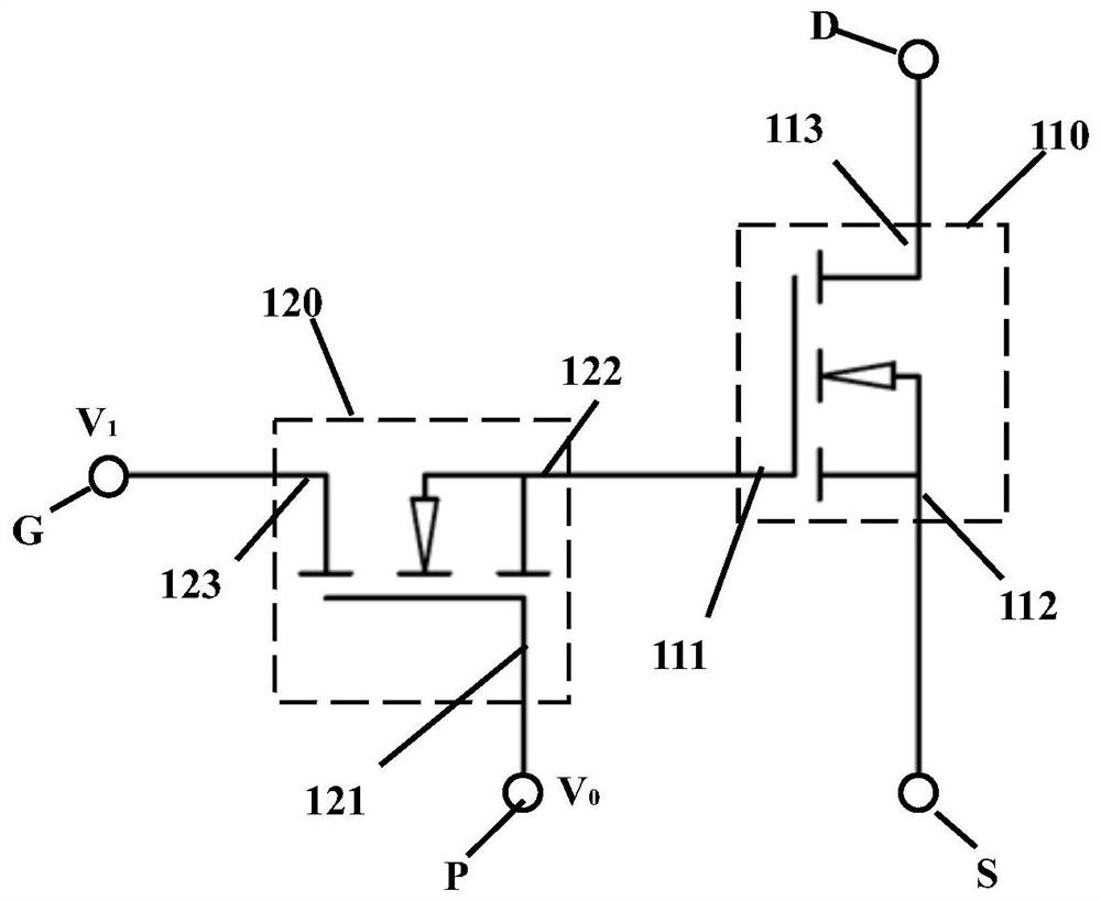
[0036] ginseng figure 1 As shown, this embodiment discloses a semiconductor circuit based on gate protection. The semiconductor circuit includes an integrated enhanced power device 110 and an enhanced device 120. The enhanced power device 110 includes a first gate 111, a second A source 112 and a first drain 113, the enhanced device 120 includes a second gate 121, a second source 122 and a second drain 123, and the first gate 111 is electrically connected to the second source 122, The first drain 113 is used as the drain D of the semiconductor circuit, the first source 112 is used as the source S of the semiconductor circuit, the second drain 123 is used as the grid G ​​of the semiconductor circuit, and the second grid 121 is used as a protective electrode of the semiconductor circuit p.

[0037] Preferably, the enhanced power device is a group III nitride enhanced power device, and the enhanced device is a group III nitride enhanced device; specifically, the enhanced power d...

Embodiment 2

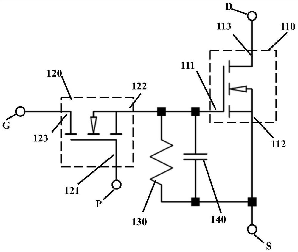
[0042] ginseng figure 2 As shown, this embodiment discloses a semiconductor circuit based on gate protection. The semiconductor circuit includes an integrated enhanced power device 110 and an enhanced device 120, and an electrical connection between the first source and the first gate. A resistor 130 and a capacitor 140 between the poles. The integration manner of the enhanced power device 110 and the enhanced device 120 is exactly the same as that in Embodiment 1, and will not be repeated here.

[0043] The resistor 130 and the capacitor 140 in this embodiment may be independent passive devices, or may be monolithically integrated with the enhanced power device 110 and / or the enhanced device 120, wherein the monolithically integrated resistor may be based on TaN Metal resistors such as metals, monolithically integrated capacitors can be capacitors based on metal-insulator-metal structure, and the insulating layer can use silicon nitride, silicon oxide, aluminum oxide, etc. ...

Embodiment 3

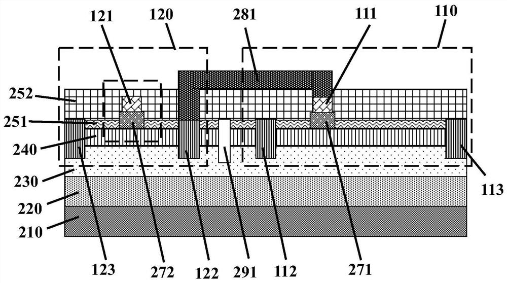
[0046] ginseng image 3 As shown, this embodiment discloses a semiconductor device based on gate protection, and the semiconductor device mainly includes an integrated enhanced power device 110 and an enhanced device 120 .

[0047] Specifically, the semiconductor device includes a substrate 210 , a first epitaxial structure and a second epitaxial structure located on the substrate and electrically isolated, several passivation layers and several electrodes located on the first epitaxial structure and the second epitaxial structure.

[0048] Wherein, the first epitaxial structure and the second epitaxial structure include a channel layer 230 located on the substrate 210 and a barrier layer 240 located on the channel layer 230. Preferably, the first epitaxial structure and the second epitaxial structure in this embodiment The epitaxial structure also includes a buffer layer 220 between the channel layer 230 and the substrate 210 .

[0049] Specifically, the substrate 210 is a c...


PUM

PropertyMeasurementUnit
Thicknessaaaaaaaaaa

Abstract

The invention discloses a semiconductor circuit based on gate protection and a semiconductor device. The semiconductor circuit comprises an enhanced power device and an enhanced device which are integrated; the enhanced power device comprises a first gate electrode, a first source electrode and a first drain electrode, and the enhanced device comprises a second gate electrode, a second source electrode and a second drain electrode; the first gate electrode is electrically connected with the second source electrode, the first drain electrode is used as a drain electrode of the semiconductor circuit, the first source electrode is used as a source electrode of the semiconductor circuit, the second drain electrode is used as a gate electrode of the semiconductor circuit, and the second gate electrode is used as a protection electrode of the semiconductor circuit. According to the invention, the gate electrode of the enhanced power device is integrated with another enhanced device, so thatthe gate electrode protection of the power device is realized; compared with an existing gate protection technology, the requirement of an external Zener diode is omitted, and the dependence on a depletion type device is removed.

Description

technical field [0001] The invention belongs to the technical field of semiconductors, and in particular relates to a gate protection-based semiconductor circuit and a semiconductor device. Background technique [0002] Gallium nitride, as a representative material of III-V compounds, has many excellent material properties such as wide energy gap, high saturation electron mobility, and high temperature resistance; at the same time, its aluminum gallium nitride / gallium nitride horizontal structure device On the premise of not relying on external doping, a high-concentration two-dimensional electron gas can be generated by the polarization effect, and high carrier concentration and high carrier mobility can be achieved at the same time; not only that, the GaN horizontal structure can also borrow It is formed on a large-size silicon wafer by epitaxial growth technology, thereby greatly reducing the cost of the device. These characteristics make GaN-based power devices switch f...

Claims


Application Information

Patent Timeline
IPC IPC(8): H01L27/088H01L29/20
CPCH01L27/088H01L29/2003
Inventor 蒋胜柳永胜胡峰白强唐瑜陈辉于洁
Owner 苏州英嘉通半导体有限公司
Learn More