Superlattice material embedded with quantum wires, preparation method of superlattice material, infrared band luminescent material and detector

A technology of infrared bands and luminescent materials, which is applied in nanotechnology for materials and surface science, semiconductor devices, and final product manufacturing. It can solve problems such as easy discovery, and achieve the effect of simple operation and obvious structural advantages

Active Publication Date: 2020-11-10
湖南科莱特光电有限公司
View PDF4 Cites 2 Cited by
  • Summary
  • Abstract
  • Description
  • Claims
  • Application Information

AI Technical Summary

Problems solved by technology

[0003] However, it is not difficult to find that at present, the quantum dot structure can only be introduced into the quantum well str

Method used


Image

  • Superlattice material embedded with quantum wires, preparation method of superlattice material, infrared band luminescent material and detector
  • Superlattice material embedded with quantum wires, preparation method of superlattice material, infrared band luminescent material and detector
  • Superlattice material embedded with quantum wires, preparation method of superlattice material, infrared band luminescent material and detector

Examples


Example Embodiment

[0062] Example 1

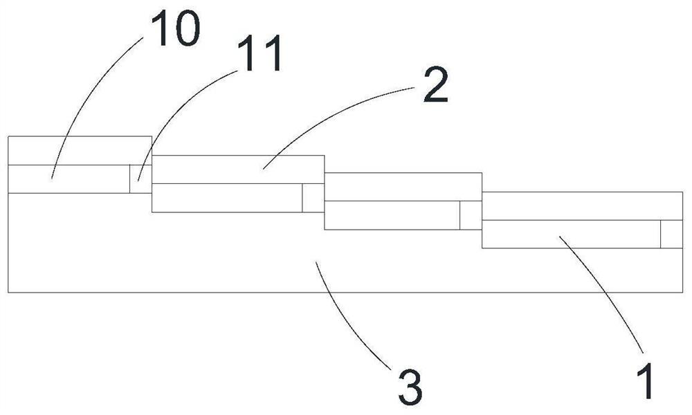
[0063] Such as figure 1 As shown, this embodiment provides a superlattice structure embedded with InAs quantum wires. The superlattice structure embedded with InAs quantum wires includes an InAs / GaSb layer 1 and a single substance layer 2. In the InAs / GaSb layer 1, the GaSb portion 10 accounts for 80%, the InAs portion 11 accounts for 20%, and the single substance layer 2 For GaSb.

[0064] The thickness of the InAs / GaSb layer 1 and the single substance layer 2 are both 10ML.

[0065] The preparation method is as follows:

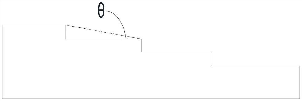
[0066] The substrate 3 is a GaSb substrate with an inclination angle, the inclination angle is 2.86°, and the step width is about 6 nm. The growth parameters include: the substrate temperature is 350°C, and the III / V beam ratio is 1:1.

[0067] Such as figure 2 As shown, the inclination angle θ represents the ratio of the height to the width of the step surface.

[0068] Growth of InAs / GaSb layer 1:

[0069] First turn on the Ga source and Sb sou...

Example Embodiment

[0082] Example 2

[0083] Reference figure 1 As shown, this embodiment provides a superlattice structure embedded with InAs quantum wires. The superlattice structure embedded in the InAs quantum wire includes an InAs / GaSb layer 1 and a single substance layer 2. In the InAs / GaSb layer 1, the GaSb portion 10 accounts for 90%, the InAs portion 11 accounts for 10%, and the single substance layer 2 For GaSb.

[0084] The thickness of the InAs / GaSb layer 1 and the single substance layer 2 are both 20ML.

[0085] The preparation method is as follows:

[0086] The substrate 3 is a GaSb substrate with an inclination angle, the inclination angle is 2.86°, and the step width is about 6 nm. The growth parameters include: the substrate temperature is 550°C, and the III / V beam ratio is 1:5.

[0087] In other embodiments, the inclination angle of the substrate can be between 1°, 2°, 3°, 4°, 5°, 6°, 7°, 8°, 9°, 10°, etc. Any value.

[0088] Growth of InAs / GaSb layer 1:

[0089] First turn on the Ga s...

Example Embodiment

[0096] Example 3

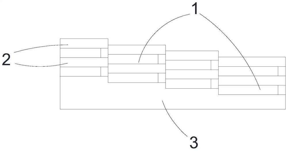
[0097] Such as Picture 11 As shown, this embodiment provides a superlattice structure embedded with GaSb quantum wires. The superlattice structure embedded in the GaSb quantum wire includes an InAs / GaSb layer 1 and a single material layer 2. InAs / GaSb layer 1 InAs part 11 accounts for 90%, GaSb part 10 accounts for 10%, and single material layer 2 For InAs.

[0098] The thickness of the InAs / GaSb layer 1 and the single substance layer 2 are both 10ML.

[0099] The preparation method is as follows:

[0100] The substrate 3 is a GaSb substrate with an inclination angle, the inclination angle is 2.86°, and the step width is about 6 nm. The growth parameters include: the substrate temperature is 150°C, and the III / V beam ratio is 1:3.

[0101] In other embodiments, the substrate 3 may be any one of a GaAs substrate, an InAs substrate, an InP substrate, and a Si substrate.

[0102] Growth of InAs / GaSb layer 1:

[0103] First turn on the In source and As source, observe t...


PUM


Abstract

The invention provides a superlattice material embedded with quantum wires, a preparation method of the superlattice material, an infrared band luminescent material and a detector. The superlattice material embedded with the quantum wires comprises at least one InAs/GaSb layer and at least one single substance layer which are arranged in a stacked mode. The InAs/GaSb layer comprises an InAs part and a GaSb part, and the single substance layer comprises InAs or GaSb; the InAs portions and the GaSb portions are alternately arranged and have different widths along the arrangement direction. The preparation method of the superlattice material embedded with the quantum wire comprises the step of sequentially growing the InAs/GaSb layer and the single substance layer on the substrate according to the structure. An infrared band light emitting material includes a superlattice material in which quantum lines are embedded. A detector comprises an infrared band luminescent material. According tothe superlattice material embedded with the quantum lines, the quantum lines are introduced into the II-type superlattice to form a line superlattice composite structure, the working temperature of adevice can be improved, and the photoelectric property of the material is improved.

Description

Technical field [0001] The invention relates to the field of semiconductors, in particular to a superlattice material embedded with quantum wires and a preparation method thereof, an infrared wave band luminescent material and a detector. Background technique [0002] III-V semiconductors, as important semiconductor optoelectronic materials, have attracted much attention in recent years. Based on their lasers with different energy band structures, detectors have shown great application prospects in the fields of national defense and civilian use, and they have achieved great results in recent years. Great research progress. Further optimizing the quantum structure of III-V semiconductors and improving the optoelectronic properties of materials will play an important role in promoting the performance of optoelectronic devices. [0003] However, it is not difficult to find that the quantum dot structure can only be introduced into the quantum well structure based on the I-type band ...

Claims


Application Information

Patent Timeline
IPC IPC(8): H01L31/0352H01L31/0304H01L31/101H01L31/18H01L33/00H01L33/04H01L33/06H01L33/30B82Y30/00B82Y40/00
CPCH01L33/06H01L33/30H01L33/04H01L33/0062H01L31/035236H01L31/035227H01L31/0304H01L31/101H01L31/184B82Y30/00B82Y40/00Y02P70/50
Inventor 杜鹏
Owner 湖南科莱特光电有限公司
Why Eureka
Try Eureka