Polycrystalline self-doped smooth top gate JFET device and manufacturing method thereof
A self-doping and smoothing technology, used in semiconductor/solid-state device manufacturing, semiconductor devices, electrical components, etc., can solve problems such as difficulties for designers, improve the ability to accurately control threshold voltage, and improve device consistency.
- Summary
- Abstract
- Description
- Claims
- Application Information
AI Technical Summary
Problems solved by technology
Method used
Image
Examples
Embodiment 1
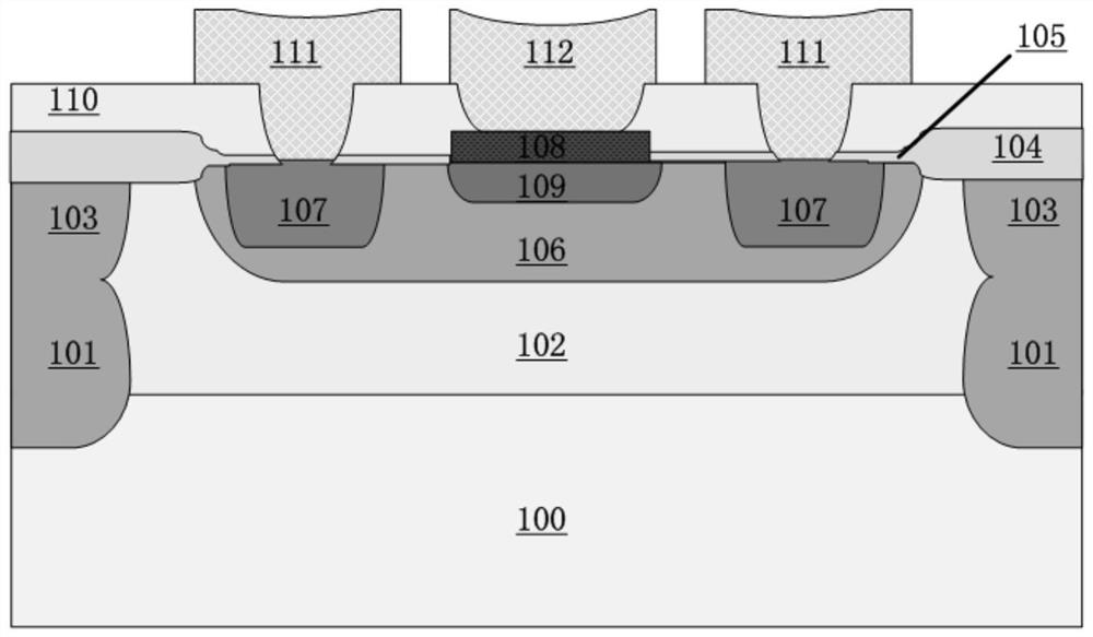
[0078] see Figure 1 to Figure 9 , a polycrystalline self-doped smooth top-gate JFET device, comprising a P-type substrate 100, a P-type buried layer 101, an N-type epitaxial layer 102, a P-type isolation penetration region 103, a field oxygen layer 104, and a pre-oxidation layer 105 , P-type channel region 106, P-type heavily doped source and drain region 107, polycrystalline gate region 108, N-type gate diffusion region 109, TEOS (orthoethyl silicate) metal pre-dielectric layer 110, source and drain first layer metal 111 and gate first layer metal 112 .
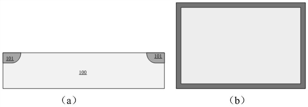
[0079] A P-type buried layer 101 is deposited on both ends of the upper surface of the P-type substrate 100 .
[0080] The materials of the P-type substrate 100 and the N-type epitaxial layer 103 include bulk silicon, silicon carbide, gallium arsenide, indium phosphide or silicon germanium.
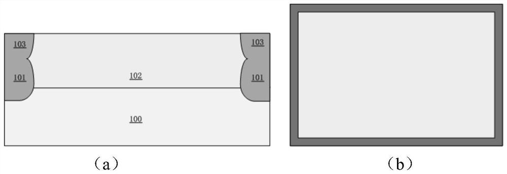
[0081] The N-type epitaxial layer 102 covers the P-type substrate 100 .
[0082] Both ends of the N-type epitaxial layer 102 are i...
Embodiment 2
[0108] A polycrystalline self-doped smooth top-gate JFET device, comprising an N-type substrate 100, an N-type buried layer 101, a P-type epitaxial layer 102, an N-type isolation penetration region 103, a field oxygen layer 104, a pre-oxidation layer 105, N-type channel region 106, N-type heavily doped source and drain regions 107, polycrystalline gate region 108, P-type gate diffusion region 109, TEOS metal front dielectric layer 110, source and drain first layer metal 111 and gate first layer metal 112 .
[0109] An N-type buried layer 101 is deposited on both ends of the upper surface of the N-type substrate 100 .
[0110] The materials of the N-type substrate 100 and the P-type epitaxial layer 103 include bulk silicon, silicon carbide, gallium arsenide, indium phosphide or silicon germanium.
[0111] The P-type epitaxial layer 102 covers the N-type substrate 100 .
[0112] Both ends of the P-type epitaxial layer 102 are in contact with the N-type buried layer 101 .
[0...
Embodiment 3
[0138] Such as figure 1 As shown, a polycrystalline self-doped smooth top-gate JFET device includes a P-type substrate 100, a P-type buried layer 101, an N-type epitaxial layer 102, a P-type isolation penetration region 103, a P-type channel region 106, P-type heavily doped source-drain region 107, polycrystalline gate region 108, N-type gate diffusion region 109, pre-oxidation layer 105, field oxygen layer 104, TEOS metal pre-dielectric layer 110, source-drain first layer metal 111, gate Pole first layer metal 102.
[0139] The P-type buried layer 101 is located at both ends of the upper surface of the P-type substrate 100 .
[0140] The N-type epitaxial layer 102 is located on the P-type substrate 100 , and the N-type epitaxial layer 102 is in contact with the P-type substrate 100 and the P-type buried layer 101 .
[0141] The P-type isolation penetration region 103 is in contact with both ends of the N-type epitaxial layer 102 , and the bottom of the P-type isolation pene...
PUM
| Property | Measurement | Unit |
|---|---|---|
| thickness | aaaaa | aaaaa |
| electrical resistivity | aaaaa | aaaaa |
| thickness | aaaaa | aaaaa |
Abstract
Description
Claims
Application Information


