A method for manufacturing a guide plate mems probe structure
A manufacturing method and guide plate technology, which are applied in semiconductor bare core testing and related key technologies, micro-electromechanical system manufacturing, guide plate MEMS probe structure manufacturing, and can solve problems such as impracticability, probe bending, and manufacturing failure. , to achieve the effect of manufacturing
- Summary
- Abstract
- Description
- Claims
- Application Information
AI Technical Summary
Problems solved by technology
Method used
Image

Examples
specific Embodiment approach 1
[0073] The following is an embodiment of a MEMS probe card.
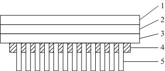
[0074] The structure diagram of the MEMS probe card under this embodiment is as follows figure 1 As shown, the MEMS probe card includes a reinforcement member 1, a PCB board 2, an adapter layer 3, a guide plate 4, and a MEMS probe 5 from top to bottom; the reinforcement member 1 is used to increase the strength of the MEMS probe card , the PCB board 2 is used to connect the testing machine and signal routing, the transfer layer 3 is the medium between the PCB board 2 and the MEMS probe 5, and is used to realize the fixed transfer of signals, and the guide board 4 is used for For accommodating MEMS probes 5, the MEMS probes 5 are used to connect the wafer under test to realize the test of the electrical properties of the wafer;
[0075] The guide plate 4 and the MEMS probe 5 jointly form a guide plate MEMS probe structure, and the guide plate MEMS probe structure is made by using a guide plate MEMS probe structure t...
specific Embodiment approach 2
[0077] The following is the embodiment of the template burning device for the guide plate MEMS probe structure.
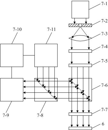
[0078] The guide plate MEMS probe structure template burning equipment under this embodiment, the structure schematic diagram is as follows figure 2 As shown, the guide plate MEMS probe structure template burning equipment is sequentially provided with a light source 7-1, a pinhole 7-2, a collimating mirror 7-3, an x-direction slit expansion plate 7-4, y-direction slit expansion plate 7-5, first prism 7-6, plane mirror 7-7, second prism 7-8, first image sensor 7-9, controller 7-10 and laser array 7-11 ;
[0079] The light beam emitted by the light source 7-1 passes through the pinhole 7-2 to form a point light source, the pinhole 7-2 is located at the focal point of the collimating mirror 7-3, and the point light source passes through the collimating mirror 7-3 to form parallel light, The parallel light passes through the x-direction slit expansion plate 7-4 to ...
specific Embodiment approach 3
[0081] The following is the embodiment of the template burning device for the guide plate MEMS probe structure.
[0082] The guide plate MEMS probe structure template burning equipment under this embodiment, the structure schematic diagram is as follows figure 2 As shown, the guide plate MEMS probe structure template burning equipment is further defined on the basis of the second embodiment:
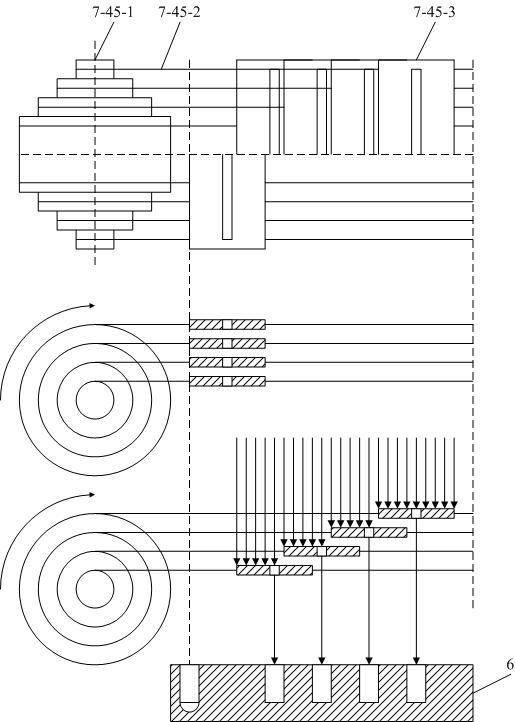
[0083] The x-direction slit expansion plate 7-4 and the y-direction slit expansion plate 7-5 are placed vertically, and both the x-direction slit expansion plate 7-4 and the y-direction slit expansion plate 7-5 include coaxial step rollers 7 -45-1, pull wire 7-45-2 and slit plate 7-45-3, the coaxial ladder roll 7-45-1, such as image 3 shown;
[0084] The coaxial stepped roller 7-45-1 includes coaxially arranged rollers with different diameters, the diameters of the rollers are arranged from small to large, which is an arithmetic sequence, and the first item is twice the tolerance, an...
PUM
 Abstract
Description
Claims
Application Information
 - R&D
- Intellectual Property
- Life Sciences
- Materials
- Tech Scout
- Unparalleled Data Quality
- Higher Quality Content
- 60% Fewer Hallucinations
Browse by: Latest US Patents, China's latest patents, Technical Efficacy Thesaurus, Application Domain, Technology Topic, Popular Technical Reports.
© 2025 PatSnap. All rights reserved.Legal|Privacy policy|Modern Slavery Act Transparency Statement|Sitemap|About US| Contact US: help@patsnap.com