Mask plate and manufacturing method thereof

A mask and mask technology, which is applied in the semiconductor field, can solve the problems of poor mask quality and achieve the effects of superior structural performance, high wear resistance, and long service life

Pending Publication Date: 2020-11-24
CHANGXIN MEMORY TECH INC
View PDF6 Cites 2 Cited by
  • Summary
  • Abstract
  • Description
  • Claims
  • Application Information

AI Technical Summary

Problems solved by technology

[0004] However, the quality of the masks provided by the prior art is poor

Method used


Image

  • Mask plate and manufacturing method thereof
  • Mask plate and manufacturing method thereof
  • Mask plate and manufacturing method thereof

Examples


Embodiment Construction

[0019] It can be seen from the background art that the quality of the mask plate provided by the prior art is relatively poor.

[0020] The analysis found that if impurities are attached to the mask, the pattern of the impurities will be transferred to the wafer, thereby affecting the performance and yield of devices fabricated on the wafer.

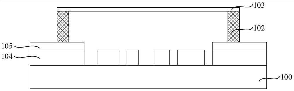
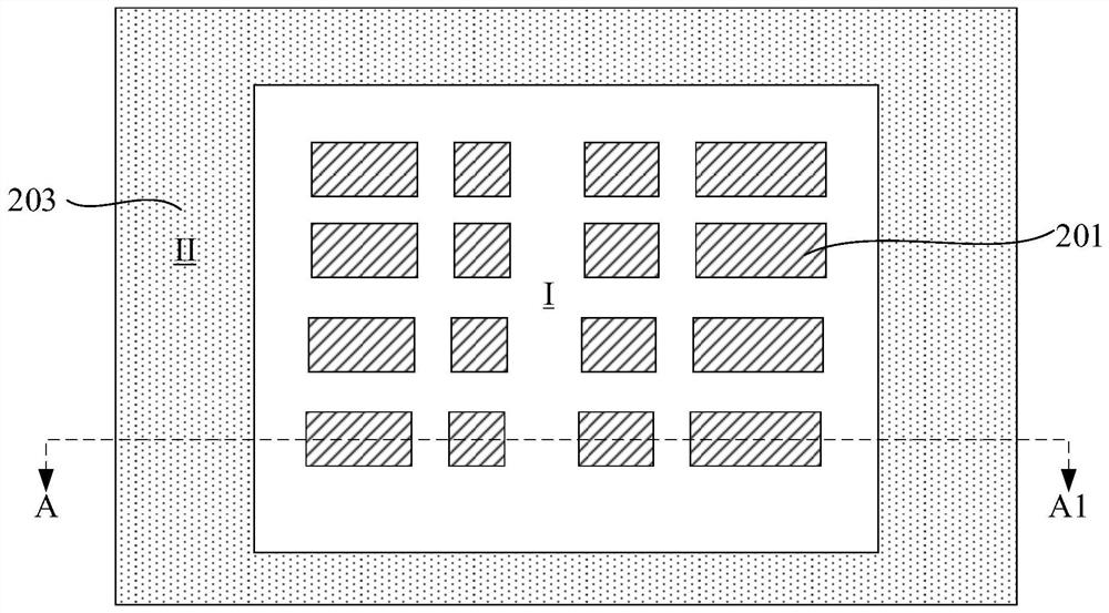
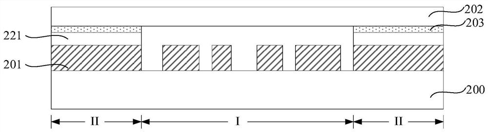
[0021] In order to better protect the mask during use and reduce the probability of impurities appearing on the mask, a mask that can prevent impurities from adhering is proposed. figure 1 is a schematic diagram of the cross-sectional structure of a mask, refer to figure 1 , the mask plate includes: a substrate 100 and a pattern metal layer on the substrate 100, the pattern metal layer includes a pattern area (not marked) and a peripheral area (not marked) surrounding the pattern area; a frame (frame) 102, the frame 102 It is located on the pattern metal layer of the peripheral area and surrounds the pattern area; a transparent film (pe...


PUM

PropertyMeasurementUnit
thicknessaaaaaaaaaa
thicknessaaaaaaaaaa

Abstract

The embodiment of the invention relates to a mask plate and a manufacturing method thereof. The mask plate comprises: a substrate; a pattern layer which is located on the substrate, wherein the pattern layer comprises a pattern area and a peripheral area surrounding the pattern area; a light-transmitting cover plate which is arranged on the peripheral area, wherein a mask cavity is defined by thelight-transmitting cover plate, the substrate and the peripheral area, and the pattern area is located in the mask cavity. The quality of the mask plate can be remarkably improved, and the service life of the mask plate is prolonged.

Description

technical field [0001] The invention relates to the technical field of semiconductors, in particular to a mask plate and a manufacturing method thereof. Background technique [0002] Graphical technology is one of the commonly used technologies in the field of integrated circuit manufacturing. An important link in the patterning technology includes the use of a mask containing circuit design information for photolithography to transfer the circuit design information to the wafer. The mask is also called photolithography. Offset, photolithography mask or photomask. [0003] The mask plate includes a substrate with light transmittance to the exposure light and a graphic layer on the substrate. The graphic layer includes at least one geometric figure with light shielding properties to the exposure light, which can selectively block the light that is irradiated onto the wafer surface. The light on the photoresist (PR) finally forms a corresponding pattern on the photoresist on...

Claims


Application Information

Patent Timeline
Patent Type & Authority Applications(China)
IPC IPC(8): G03F1/38
CPCG03F1/38
Inventor 不公告发明人
Owner CHANGXIN MEMORY TECH INC
Why Eureka
Try Eureka