Electronic substrate, connector assembly and manufacturing method of electronic substrate

An electronic substrate and manufacturing method technology, applied in the direction of electrical connection of printed components, connections, electrical components, etc., can solve the problems of cumbersome processing methods, signal jitter, peeling, etc., to ensure continuity and stability, reduce loss, and ensure The effect of transmission

Active Publication Date: 2020-11-24
DEYI PRECISION ELECTRONIC IND CO LTD PANYU
View PDF11 Cites 4 Cited by
  • Summary
  • Abstract
  • Description
  • Claims
  • Application Information

AI Technical Summary

Problems solved by technology

However, since the PTFE plate and the conductive plate need to be roughened first, the treatment method is cumbersome, and the concave parts on the roughened surface of PTFE and the convex parts on the roughened surface of the conductive plate are not necessarily set opposite to each other. , so that the bonding force between the two is reduced, which in turn causes the conductive sheet to be easily peeled off from the surface of the PTFE sheet; and because the concave and convex parts are unevenly distributed on the conductive sheet, the conductive path is transmitted on the conductive sheet and passes through the concave and convex When the part is exposed, it is easily affected by the concave and convex parts, which makes the signal jitter during transmission, which in turn affects the quality and rate of signal transmission
[0004] Therefore, in order to solve the problem of unstable bonding between the concave-convex part on the conductive plate and the concave-convex part on the polytetrafluoroethylene plate and the influence of the uneven concave-convex part on the conductive plate on signal transmission, it is necessary to design a new An electronic substrate of polytetrafluoroethylene material and conductive material and a connector assembly with the new electronic substrate, and the new electronic substrate is produced by a new manufacturing method

Method used


Image

  • Electronic substrate, connector assembly and manufacturing method of electronic substrate
  • Electronic substrate, connector assembly and manufacturing method of electronic substrate
  • Electronic substrate, connector assembly and manufacturing method of electronic substrate

Examples


Embodiment Construction

[0054] In order to facilitate a better understanding of the purpose, structure, features, and effects of the present invention, the present invention will now be further described in conjunction with the accompanying drawings and specific embodiments.

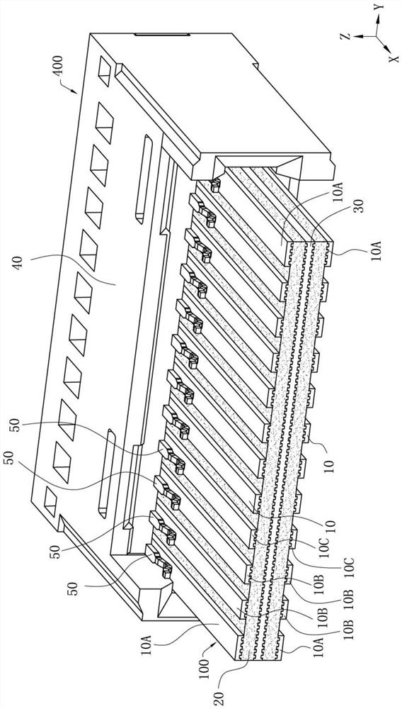
[0055] In this specific embodiment, the forward direction in the front-rear direction is defined as the positive direction of the X-axis, the leftward direction in the left-right direction is defined as the positive direction of the Y-axis, and the upward direction in the up-down direction is defined as the positive direction of the Z-axis .

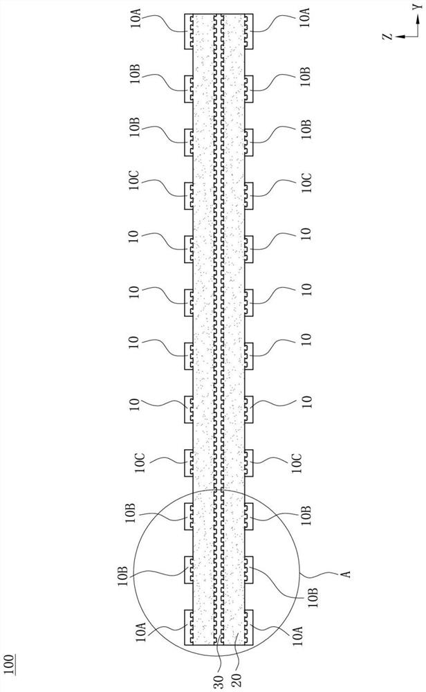
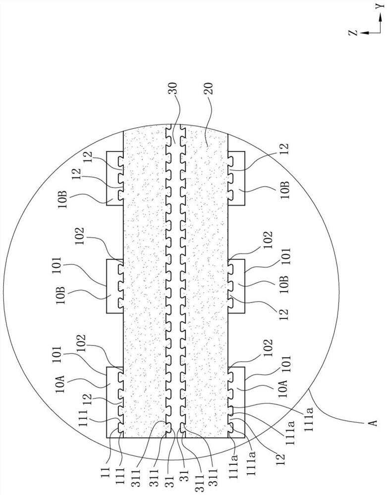
[0056] Such as Figure 1 to Figure 8 As shown, it is a connector assembly according to Embodiment 1 of the present invention. The connector assembly includes an electronic substrate 100 and an electrical connector 400 electrically connected to the electronic substrate 100. One end of the electronic substrate 100 is along the front and rear Direction is plugged into the electrical connect...


PUM


Abstract

The invention discloses an electronic substrate. The electronic substrate comprises a polytetrafluoroethylene base layer and a plurality of conductive strips arranged on the polytetrafluoroethylene base layer, each conductive strip is provided with a first surface and a second surface which are opposite up and down, wherein at least one groove is concavely formed from the second surface to the first surface; the grooves do not penetrate through the conductive strips in the vertical direction; the grooves extend along the front-back direction, the polytetrafluoroethylene base layer partially fills the grooves, the groove walls of the grooves are provided with at least one stopping surface, the stopping surface prevents the part, filling the grooves, of the polytetrafluoroethylene base layerfrom being separated from the conductive strips in the direction opposite to the concave direction of the grooves, and a conductive path of the conductive strip is defined to transmit signals in thefront-back direction. Compared with the prior art, the polytetrafluoroethylene material and the conductive material in the electronic substrate are tightly combined, loss can be reduced when signals are transmitted on the conductive strip, and transmission is stable.

Description

【Technical field】 [0001] The present invention relates to an electronic substrate, a connector assembly and a manufacturing method of the electronic substrate, in particular to an electronic substrate with a polytetrafluoroethylene-based material and a conductive material, a connector assembly with the electronic substrate, and the electronic substrate. Production Method. 【Background technique】 [0002] Polytetrafluoroethylene (PTFE), commonly known as Teflon, is widely used in the electronic substrate industry due to its small dielectric constant, small dielectric loss, and high breakdown voltage. However, the surface energy of the polytetrafluoroethylene material is extremely low, and it is not easy to bond with conductive materials, so it is difficult to form a conductive layer on the surface of the polytetrafluoroethylene material to realize the transmission of electrical signals. [0003] At present, the combination method usually used between polytetrafluoroethylene m...

Claims


Application Information

Patent Timeline
Patent Type & Authority Applications(China)
IPC IPC(8): H01B7/00H01B7/04H01B7/08H01B11/00H01B13/00H05K1/02H05K1/11H05K3/00H01R12/77
CPCH01B7/0009H01B7/04H01B7/0846H01B7/0861H01B11/00H01B13/00H05K1/118H05K1/0213H05K3/00H01R12/77
Inventor 蔡侑伦
Owner DEYI PRECISION ELECTRONIC IND CO LTD PANYU
Why Eureka
Try Eureka