Trench gate of trench type device preparation method and trench gate of trench type device
A trench gate, trench type technology, applied in the manufacture of semiconductor/solid state devices, semiconductor devices, electrical components, etc., can solve the problem of low breakdown voltage at the top corner of the trench, easy breakdown of trench type devices, and electric field breakdown. Breakdown and other problems, to achieve high breakdown voltage, reduce the probability of failure, and improve the effect of breakdown voltage
- Summary
- Abstract
- Description
- Claims
- Application Information
AI Technical Summary
Problems solved by technology
Method used
Image
Examples
Embodiment 1
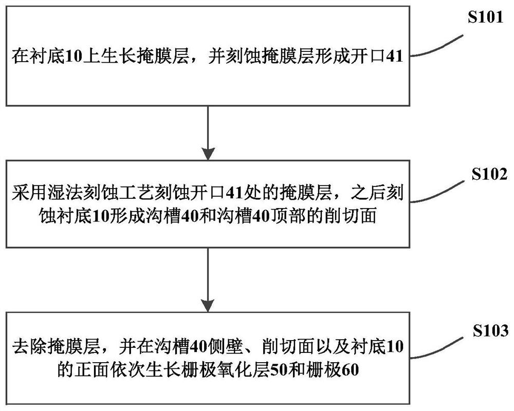
[0050] Embodiment 1 of the present invention provides a method for preparing a trench gate of a trench type device, and the specific flow chart is as follows figure 1 As shown, the specific process is as follows:
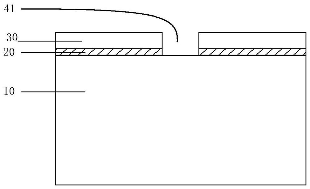
[0051] S101: growing a mask layer on the substrate 10, and etching the mask layer to form an opening 41;
[0052]S102: Etch the mask layer at the opening 41 by using a wet etching process, and then etch the substrate 10 to form the trench 40 and the chamfered surface at the top of the trench 40;
[0053] S103 : remove the mask layer, and sequentially grow the gate oxide layer 50 and the gate 60 on the sidewall of the trench 40 , the cut surface and the front surface of the substrate 10 .
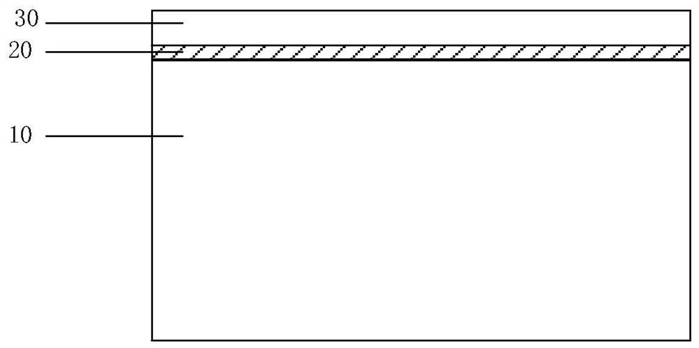
[0054] Growing a mask layer on the substrate 10, and etching the mask layer to form an opening 41, including:
[0055] The substrate 10 is cleaned by a wet cleaning process; in Embodiment 1 of the present invention, the substrate 10 adopts a silicon substrate, and the substrate ...
Embodiment 2
[0078] Embodiment 2 of the present invention provides a trench gate prepared by a method for preparing a trench gate of a trench type device, such as Figure 9 As shown, it includes a gate oxide layer 50 and a gate 60, and the gate 60 is located on the front side of the gate oxide layer 50;
[0079] The gate oxide layer 50 and the gate 60 are sequentially grown on the sidewall of the trench 40, the cut surface and the front surface of the substrate 10, and the trench 40 and the cut surface at the top of the trench 40 are etched at the opening 41 by using a wet etching process. The mask layer is formed by etching the substrate 10; the opening 41 is formed by growing a mask layer on the substrate 10 and etching the mask layer.
[0080] For the convenience of description, each part of the device described above is divided into various modules or units by function and described separately. Of course, when implementing the present application, the functions of each module or unit ...
PUM
| Property | Measurement | Unit |
|---|---|---|
| thickness | aaaaa | aaaaa |
| thickness | aaaaa | aaaaa |
Abstract
Description
Claims
Application Information


