
Preparation method and structure of overlay alignment mark

An alignment mark and marking technology, applied in electrical components, electrical solid devices, circuits, etc., can solve the problems of large capital investment in lithography equipment, measurement error of overlay alignment marks, and lithography step errors, etc. Improve lithography accuracy, reduce measurement errors, and improve signal strength

Active Publication Date: 2020-12-01
SIEN QINGDAO INTEGRATED CIRCUITS CO LTD
View PDF7 Cites 2 Cited by
  • Summary
  • Abstract
  • Description
  • Claims
  • Application Information

AI Technical Summary

Problems solved by technology

[0005] At present, for the measurement of the overlay alignment mark on the back, the infrared measurement method is usually used, but when the back is aligned, the signal strength of the front mark in the overlay alignment mark to the infrared ray is weak, which is easy to cause overlay alignment. The measurement error of the quasi-mark will cause errors in the photolithography step, resulting in product failure
[0006] In order to improve the overlay alignment accuracy, people have obtained partial satisfaction by improving lithography equipment, but the improvement and replacement of lithography equipment requires a large capital investment, resulting in a waste of funds

Method used


Image

  • Preparation method and structure of overlay alignment mark
  • Preparation method and structure of overlay alignment mark
  • Preparation method and structure of overlay alignment mark

Examples


Embodiment Construction

[0047] Embodiments of the present invention are described below through specific examples, and those skilled in the art can easily understand other advantages and effects of the present invention from the content disclosed in this specification. The present invention can also be implemented or applied through other different specific implementation modes, and various modifications or changes can be made to the details in this specification based on different viewpoints and applications without departing from the spirit of the present invention.

[0048] see Figure 1 to Figure 10 . It should be noted that the diagrams provided in this embodiment are only schematically illustrating the basic idea of ​​the present invention, and only the components related to the present invention are shown in the diagrams rather than the number, shape and shape of the components in actual implementation. Dimensional drawing, the type, quantity and proportion of each component can be changed ar...


PUM


Abstract

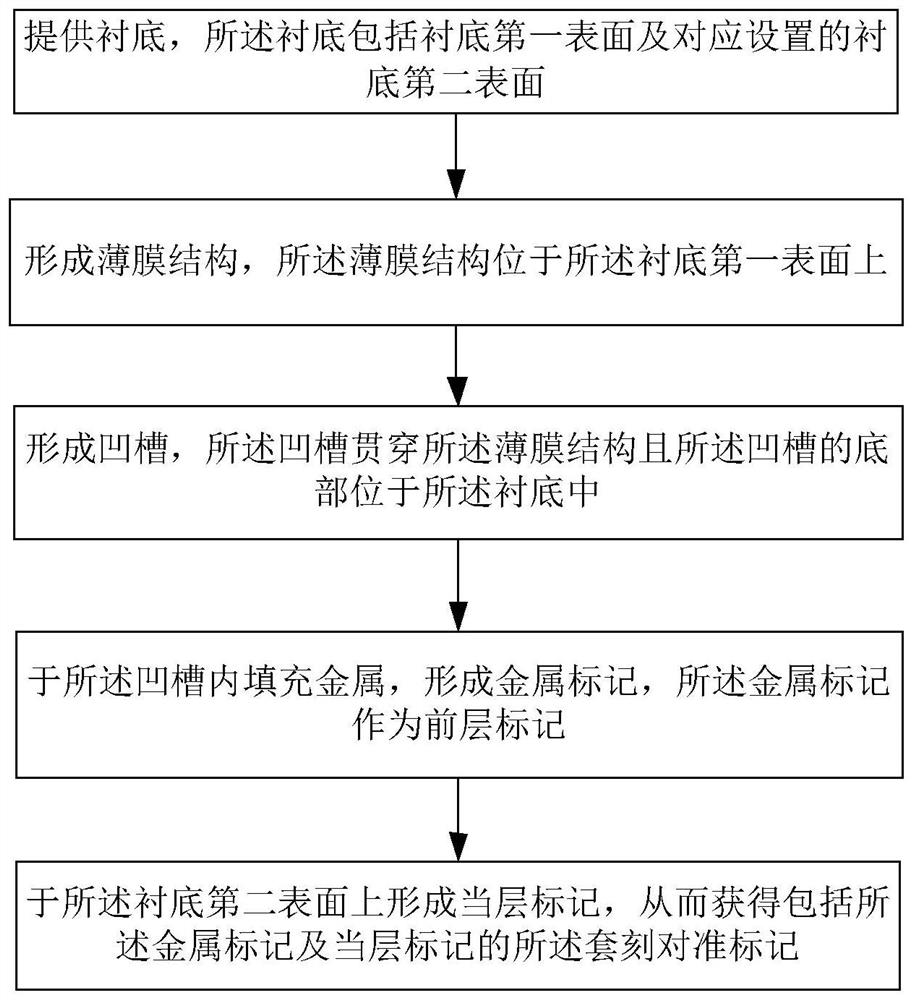
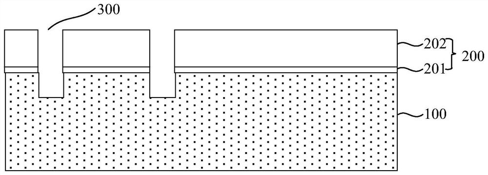
The invention provides a preparation method and a structure of an overlay alignment mark. The overlay alignment mark comprises a metal mark and a current layer mark, wherein the metal mark serves as afront layer mark, the metal mark penetrates through the thin film structure, the bottom of the metal mark is located in the substrate, the substrate comprises a substrate first surface and a substrate second surface arranged correspondingly, and the thin film structure is located on the substrate first surface; the layer mark is located on the second surface of the substrate. According to the invention, the metal mark is used as the front layer mark, so that the signal intensity of the front layer mark to infrared rays is improved, the measurement error of the overlay alignment mark is reduced, the OVL is improved, the photoetching precision is improved, and the product quality is improved, and the metal marks are formed while the metal interconnection structure is formed, so that the cost can be further reduced.

Description

technical field [0001] The invention relates to the technical field of semiconductors, in particular to a method for preparing an overlay alignment mark and its structure. Background technique [0002] The manufacture of integrated circuit chips, from a structural point of view, is similar to building a house. It starts from the substrate and builds up layer by layer. A certain degree of precision alignment must be ensured between layers, so as to ensure the normal function of the final chip. We define the layer-to-layer alignment metric as the registration accuracy (overlay, OVL). [0003] Registration accuracy and critical dimensions are the basic measurement indicators of the lithography process. The critical dimensions ensure the required line width on the chip, and the registration accuracy ensures the alignment of the lines between different layers. To put it simply, OVL is the alignment accuracy between the current layer and the previous layer in the lithography proc...

Claims


Application Information

Patent Timeline
Patent Type & Authority Applications(China)
IPC IPC(8): H01L23/544
CPCH01L23/544
Inventor 曹海东
Owner SIEN QINGDAO INTEGRATED CIRCUITS CO LTD
Learn More